


Inspired by several videos and lectures from American and German universities, such as those at the Perdue University, the University of California Berkeley, Stanford University, Massachusetts Institute of Technology (MIT) Ohio University, Indian Institute of Technology Delhi, and the Free University of Berlin (FU Berlin). All these courses are characterized by clarity, quality, and a practical, research-oriented approach. I recommend watching the videos provided here instead of searching for them on the internet yourself. It is also a good opportunity to improve your English.
Advanced Electrochemical Solar Energy Conversion to green Hydrogen and Carbone Dioxide reduction: Learning from the nature
Summary - A close look to the figure 1 shows that Hydrogen technology is intensively used for refining and chemicals. However, 95% of the its production is coming from steam reforming of natural gas, which are emitting 830 million tons/year of CO2.

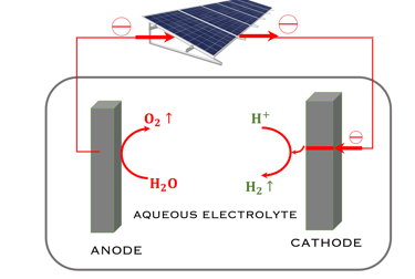
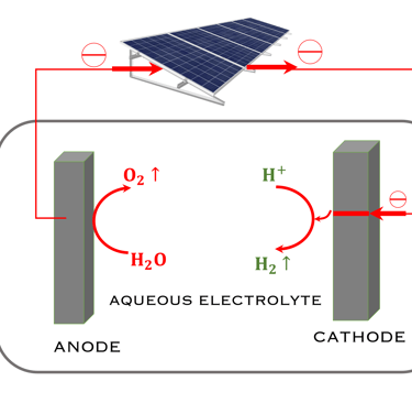
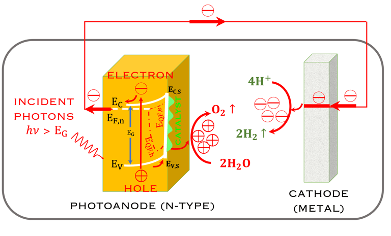
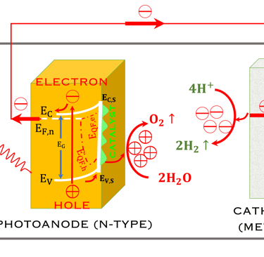
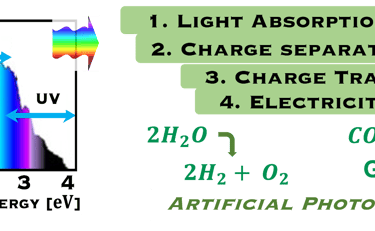
The environmental impact is challenging for large-scale development. Obviously the use of renewable energy resources can offer zerro emission of greenhouse gases and become the sustainable solution of the future. Inspired from the nature, “thanks to the photosynthesis process by which plants convert sunlight and water into energy” we will deeply discuss the process of "Photoelectrochemical solar energy conversion" and the conditions to achive efficient solar-to-hydrogen devices. Firstly, we describe a photoelectrochemical Solar cell (PEC) in the dark and under illumination. PEC consists of two photoactive semiconductors working electrodes (n and p-type) immersed in the electrolyte containing suitable aqueous redox electrolyte. The illumination (see Figure 2) of the semiconductor/electrolyte junction with a light having energy greater than the band gap (𝐸𝐺) of the semiconductor, we can observe a process similar to the photosynthesis, namely: (1) Light absorption; (2) Charge separation; (3) Charge transport; (4) Electricity and/or fuel generation. Upon light excitation, charge carriers (electrons and holes), are generated within the semiconductors. The minority carriers are separated in the space region by the electrical field and move to the Solid/Liquid interfaces. Holes migrate to the n-type semiconductor photoanode surface to complete oxidation of water, the resulting hydrogen protons move to the cathode through a membrane and reduced by the photogenerated electrons at the surface of the p-type photocathode liberating green hydrogen (𝐻2). This is a direct way to convert solar energy into fuels and requires an amount of Gibbs free energy ∆𝐺 = 238 𝑘𝐽/𝑚𝑜𝑙 reaction:
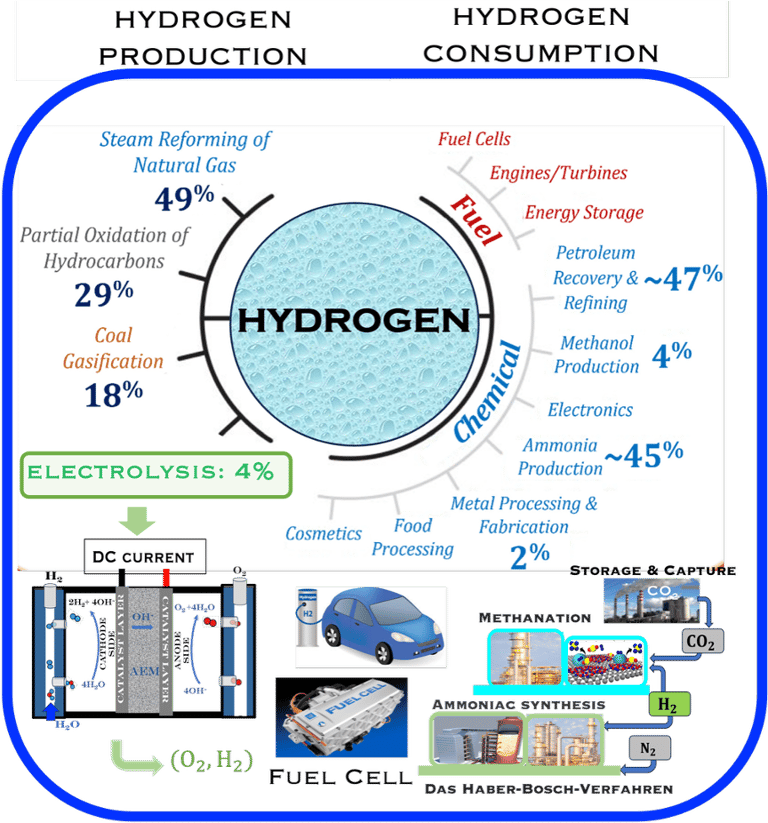
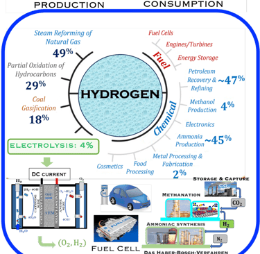
Figure 1: Powe to X, showing hydrogen production and consumption adapted from: S. Shiva Kumar and Hankwon Lim, Energy Reports 8 (2022), pp. 13793-13813 entitled An overview of water electrolysis technologies for green hydrogen production. Only ca. 4% of hydrogen production represents green hydrogen from water splitting using DC electrical energy. The illustration shows a complete scenario of carbon capture utilisation and storage solutions for different industries (e.g. Haber–Bosch process) . The highlight includes hydrogen car and fuel cells
We have to keep in mide the photoelectrodes must possess an energy gap (Eg) exceeding the thermodynamic limit of 1.23 eV. Also, the electron transfer occurs via a single electron process (one photon excites one electron per time). However, the (photo)electrochemical water splliting (4 electrons process) goes through a multistep requires favourable electrocatalyst activities of the photoelectrodes with favorable kinetics to allow such complex OER and HER reactions. As a matter of semiconductores with photocatalystic performance necessary to achieve the goal, namely: high solar-to-hydrogen energy conversion efficiency. The attendees should be:
1) Able to understand the fundamental concepts of semiconductor/Electrolyte junction
2) Able to recognize the differences between metal and semiconductor electrode materials;
3) Able to identify and explain all processes that occur at Solid/Electrolyte interface namely: majority/minority carriers, charge generation/recombination, band bending, flat band potential, surface states, band shifts, and Fermi Level pinning
4) Able to perfome Curren-Voltage and capacitance measurements
5) design catalysts in material sciences
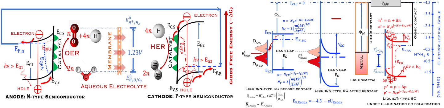
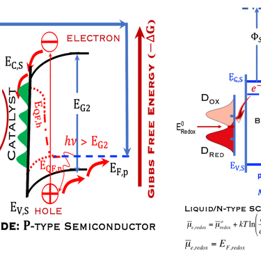
Figure 2: Left: Analogy with the “Artificial Photosynthesis Process”, namely: water splitting reactions: evolution reaction (OER) on the anode surfaces and evolution reaction (HER) on the cathode surface described in the illustration. The kinetics of (Photo)-Electrochemical electron and ion transfers depend strongly of the catalytic performance of the photo-electrodes. Right: illustration and comparison of a metal, semiconductors (n- and p-type) and redox electrolyte versus two scales (absolute scale vs. vacuum and electrochemical scale vs. Hydrogen SHE)

PROF. AHMED ENNAOUI
President of the scientific council of IRESEN
Former head of research group at Helmholtz-Zentrum Berlin für, Materialien und Energie Founder of Virtual Learning University
Biography - Ahmed Ennaoui obtained his MSc and Doctoral thesis in Solid State Electronic from "University de Bourgogne", France. He began his career as assoc. Professor ni 1979 at University Mohamed V and joined the Hahn-Meitner Institute-Berlin (HMI) in 1983 as a scientist conducting research for his Habilitation. In April 1987, he obtained his habilitation (summa cum laude) on new earth abundant materials for solar energy conversion. He works as head of a research group in the Institute for Heterogeneous Material Systems at Helmholtz - Zentrum Berlin (HZB) for materials and energy, Berlin, meanwhile, he serves in the tutorial evaluation of renewable energy seminar program for graduate students at Free University Berlin, and as visiting professor at the Research Center for Solar Energy Chemistry Osaka University, Japan. He was working as Research Director at Qatar Environmental and Energy Research Institute (QEERI) and Joint Professor at Hamad Bin Khalifa University. Ennaoui's published mostly on transition metal chalcogenide, binary and ternary thin film compounds and related solar cells. Recently he conducted research on inkjet printed thin film solar cells, and PV soiling solution. He published more than 300 scholarly contributions, including peer-reviewed research papers and numerous invited conference keynotes and proceeding papers. Recently, he is listed by Stanford University as one of the top 2% of researchers in the world out of 224, 856 researchers in applied physics ranked by the prestigious American university. Per the AD Scientific Index. He is a permanent member of the Editorial Board of Solar Energy Materials and Solar Cells, member of International Energy Society (ISES), and senior member of the Institute of Electrical and Electronic Engineers (IEEE). During his career he supervised several completed thesis, and habilitations and ca. several Postdoctoral have worked in his group. Professor Ennaoui still chairman of the scientific council of the Institute of Solar Energy and new Energy, where he has contributed to the development of renewable energies by following the completion of IRESEN's research and development projects and by organizing and participating to several international conferences in Morocco and worldwide on green energies. He is the founder of this virtual Learning university
Ladies and gentlemen.
I would like to take this opportunity to congratulate all our colleagues and friends for their intellectual contribution to this noble project. As you know that the COVID-19 pandemic in the world has affected every aspect of our society and our education system has undergone huge changes. Thus, the Virtual Learning University was born and evolved to achieve the democratization of education where education is transferred to every citizen wherever and whenever he/she wants. We have conceptualized our university according to our interest in green technology and sustainable development, exploring what is critical to strengthen research and development in order to make significant improvements and innovations in our educational system with new knowledge and skills with the aim of obtaining training in a skill and preparing a new generation for new jobs, green technologies to solve emerging issues related to sustainable development, renewable energy and environment, science and technology. Our philosophy is built on the principle of flexibility to provide learners with the necessary skills and allow them to determine what they want to learn, why, how and when to become active, responsible and engaged citizens, this is a shared responsibility to seize opportunities and find solutions
We thank you for your participation and your noble work
The Virtual Learning University (VLU) is a non-profit online educational institution founded at the beginning of the COVID-19 pandemic. A number of colleagues and friends from Moroccan, European universities and institutions, including the United States, Canada, and Turkey, voluntarily joined VLU. The platform targets engineering graduate, master's and doctoral students. We focus on deep understanding of renewable energy and energy storage; green hydrogen; climate change and global warming; water treatment and reuse; desalination technologies and other topics of interest
I'm very grateful to my colleagues for the kindness, and for the generosity they show in giving their time and support to the Virtual Learning University


Ostad Salem Rajab Zayed Omar
Executive Director of Sabaek for Education and Training, Social Programs, Human development, Scientific ResearchCenter
(Kingdom of Bahrain)
Prof. Abdelilah Benyoussef
Hassan II Academy of Sciences and Technology, Rabat, Morocco LaMCScI, Faculty of Sciences, Mohammed V University, Rabat, Morocco
Dip- Ing. Badr Ikken
Executive-President of Gi3 / Managing partner of Gi2 / Chairman of the Morocco-Germany Business Council - CGEM Member of the Board of Directors of the German Chamber of Commerce AHK Morocco
Dr. Ismail Akalay
Chief Executive Officer of Sonasid and Former general manager cobalt and base metals general manager cobalt and base metals managem

Prof. Ismael Saadoune
Ful Professor at Mohammed VI Polytechnic University, Morocco. Expert in electrochemical energy storage and batteries recycling


Prof. Saleh Khamlich
Research Centre of Excellence, UM6P - Mohammed VI Polytechnic University

Prof. Ahmed Ihlal
University Ibn Zohr, Faculty of Sciences, Agadir
Expert evaluator in the field of renewable energies for CNRST
Webinars from the Archives of Virtual Learning University
We kick off the opening of this webpage with webinars by Prof. Sabri Kais, who talks about quantitative machine learning for complex systems and quantum computing

Sabri Kais received his bachelor's, master's, and doctoral degrees from the Hebrew University of Jerusalem in 1983, 1984, and 1989, respectively. From 1989 to 1994, he worked as a research associate at Harvard University, Department of Chemistry. He then joined Purdue University in Indiana in 1994 until 2024, where he served as Distinguished Professor of Chemistry, Electrical and Computer Engineering, and Professor of Computer Science and Physics. He has published more than 290 papers in peer-reviewed scientific journals. His group's research is mainly devoted to quantum information and quantum computing for complex systems. He is a Fellow of the American Physical Society, Fellow of the American Association for the Advancement of Science, Guggenheim Fellow, Purdue University Faculty Scholar, National Science Foundation Fellow, 2012 Sigma Xi Research Award, 2019 Herbert Newby McCoy Award, Purdue
Prof. Sabre KAIS
Goodnight Distinguished Chair in Quantum computing, the department of electrical and computer engineering, North Carolina State University


Second serie of webinars by Prof. Dr. Mohammed Nazeeruddin, Professor and Director of the Laboratory of Molecular Engineering at the Federal Polytechnic University of Lausanne, Switzerland on engineering synthesis of efficient and stable perovskite solar cells

Mohammad Khaja Nazeeruddin is Professor of Chemistry at the EPFL Sion campus, and his current research at EPFL focuses on Perovskite Solar Cells and Light-emitting diodes. He has published more than 785 peer-reviewed papers, ten book chapters, and he si the inventor/co-inventor of over 90 patents. His work's high impact has been recognized by invitations to speak at over 300 international conferences. He appeared ni the ISI listing of most cited chemists and has more than 150'335 citations with an h-index of 171. He teaches the "Functional Materials" course at EPFL and Korea University. According to the Web of Science ni 2016, he is the 5th most cited chemist in the world and si one of the 19 scientists identified by Thomson Reuters as the World's Most Influential Scientific Minds in 2015. He has been named Thomson Reuters "Highly Cited Researcher" from 2014 to 2021 and listed among the Top 10 researchers in the perovskite solar cell research field by the Times Higher Education. He is directing and managing several industrial, national, and European Union projects. He has been appointed as World Class University professor by Korea University and Adjunct Professor by King Abdulaziz University, Jeddah. He has been elected to the European Academy of Sciences, Fellow of The Royal Society of Chemistry, and Fellow of Telangana Academy of Sciences and has won the 34th Khwarizmi International Award (KIA) Laureate in Fundamental Sciences, 2021.
Prof. Mohammad Khaja Nazeeruddin
Swiss Federal Institute of Technology in Lausanne, EPFL, Switzerland


Third Webinars from Prof. Dr. Thomas Hannappel, on Green hydrogen production through water splitting "ARTIFICIAL PHOTOSYNTHESIS"
Thomas Hannappel is full professor, head of the department "Fundamentals of Energy Materials", and Dean of the master course "Renewable Energy Techniques" at the Institute of Physics, Technische Universität Ilmenau. Prior of serving at Technische Universität Ilmenau, he works as scientific director at CIS Research Institute Erfurt, and acting director of the Institute “Dynamics of interfacial reactions” at the Helmholtz-Zentrum Berlin, department head at Hahn-Meitner-Institute Berlin, and lecturer at the Free University Berlin (since 2005). In 2003/04 he conducted research on silicon/III-V-heterointerfaces at NREL. He received his PhD with studies on photo-induced charge carrier dynamics performed in Prof. Gerhard Ertl's Department 'Physical Chemistry' at the Fritz-Haber-Institute Berlin. He established original analysis of semiconductor growth processes to scrutinize high-performance optoelectronic materials and complex physicochemical interfacial reactions for the development of highly efficient device structures achieving world record values for the conversion efficiency of solar cells as well as solar fuels production.

Prof. Thomas Hannappel
Head of the department “Fundamentals of Energy Materials” Dean of the Master course “Renewable Energy Techniques” at the Institute of Physics, Technische Universität (TU) Ilmenau


The second series of seminars, is presented by Prof. Evan Gordon, entitled Sustainable Silicon Photovoltaic Cell and Module Technology in the Terawatt Era

Ivan Gordon received his PhD in the field of new magnetic materials for sensor applications from the University of Leuven, Belgium in February 2002. He started working in the field of photovoltaics in June 2003 at the International Integrated Technology Center. He currently leads the photovoltaic technology and power systems group at IMO-IMOMEC. In addition, he is also a part-time professor of digital photovoltaics at Delft University of Technology in the Netherlands and editor-in-chief of the international scientific journal Solar Materials and Solar Cells. Since January 2016, he is the coordinator of the Joint Program on Photovoltaics of the European Energy Research Alliance (EERA) and a steering committee member of the European Technology and Innovation Platform for Photovoltaics. He has authored and co-authored more than 240 papers in journals and conferences (~4500 citations, Factor H36, October 2024). He is a member of the scientific committee of several international conferences (e.g. European Solar PV Conference, IEEE Solar Photovoltaics Specialists Conference, Silicon Photovoltaics Conference, International Conference on Renewable and Sustainable Energy) and has personally presented more than 30 invited lectures at international conferences, workshops and schools.

An overview will be given of the state-of-the-art of crystalline silicon (c-Si) photovoltaics (PV) by Prof. Dr. Ivan Gordon in this video
The following tasks concerns an introduction to solar energy conversion, Silicon and perovskite PV, including single junction/thin-film perovskite, perovskite/silicon tandem along with reference to the major players. and the fundamental and backgrounds on green hydrogen using photo-electrochemical conversion
Task I: Introduction to solar energy conversion
Obviously it can take more than a decade and the commitment of numerous research groups to develop a semiconductor for efficient solar energy conversion. One only has to look at the development of crystalline silicon (c-Si), which is the basis of semiconductor industry and the information technology revolution, Thank to Gordon Moore one of the founders of Intel and his famous Moore’s Law, it says the number of transistors that can be placed on an integrated circuit doubles approximately every two years. His prediction that chips with 65,000 components would be available by 1975 leads to Pentium 4 with around 55 million components per chip (2003).
Can we talk about Moore ´s law in photovoltaic technology ?
My own research for the habilitation in 1983 at Hahn-Meitner-Insitute, Berlin, Germany, I focused on the development of low cost materials for solar energy conversion as alternative to silicon [invited chapter: Iron Disulfide for solar energy conversion, Ahmed Ennaoui et al. Solar Energy Materials and Solar Cells 29 (1993) 289-370] to follow the Moore ´s law instead of sizes of transistor to become smaller, lighter, faster and consumes less energy, we thought about similar idea, a solar cell to become Thinner , Cheaper, Efficient, and lowering the production cost . Obviously, the "learning curve" (figure T.I.2 ), shows that silicon technology with increasing mass production demonstrates a decrease of the cost (USD/Wp), and demonstrate continuous increase of the efficiency, we have to keep in mind the disadvantage of high material consumption which is the main barrier when go forward to terawatt-scale, Indeed one gigawatt photovoltaic installation requires approximately 8000 tons of high quality silicon, which is a significant portion of the world production. Although silicon is abundant, a very large number of silicon production at the terawatt-scale would be necessary, including material shortages and environmental concerns. Research & development and Innovation (R&DI) to achieve the goal of terawatt-scale necessary for the energy transition worldwide. The challenge is to bring PV to grid parity without feed-in-tariffs and other subsidies


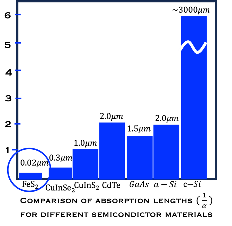
The question therefore arises as to what flexibility remains for research and development of alternative materials. There is no doubt that highly absorbing materials composed of abundant and non-toxic elements are highly desirable. As Figure T.I.3a shows, the material consumption is significantly reduced in many semiconductors thin layer compared to silicon
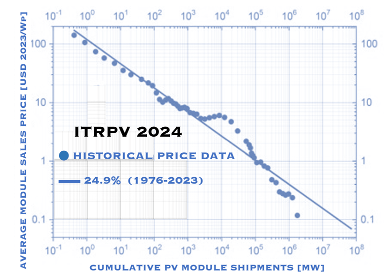
T.I.2 Learning curve, reflecting average module prices of technology (2023 US$/Wp) which decreased by 24.9% for each doubling of cumulative installed capacity (1976-2023)
Source: ITRPV and PV Magazine, JUNE 5, 2024, Sandra Enkhardt
T.I.1 Semi-log plot of transistor counts (Moor ´s law) suited to 2000, showing the number of transistors in an integrated circuit (IC) doubling about every two years
T.I.3a Left: penetration depth of light in different semiconductors. An extremely ultra-thin film of Iron dioxyde (Pyrite, Band Gap 0.9eV) is enough to absorb a large portion of the solar spectrum. (see original paper in [Ahmed Ennaoui et al. Solar Energy Materials and Solar Cells 29 (1993) 289-370] )
Task II: Introduction to solar energy conversion: PV technology evolution
Moore’s law and the solar industry development played a crucial role in the development of engineering and manufacturing of silicon. The production of metallurgical grade (MG-Si) polysilicon, typically > 98% pure silicon requires several steps de reduction and purification of the silica sand. Furthermore, the conversion of (MG- Si) is refined to produce solar and semiconductor grade polysilicon, which can be used as the feedstock for crystal growth to produce semiconductor grade single crystal silicon suitable for device manufacturing. Czochralski(CZ) growth is actually the dominant process for converting polycristalline to single-crystal Silicon ingots. The global semiconductor wafer market size was valued at USD 20.18 billion in 2022 and it is expected to hit around USD 35.16 billion by 2032 for different applications such as Renewable energy, electronics, automotive, telecommunications, healthcare industries, IoT, AI, 5G and EV, etc...


The conversion of Metallurgical grade silicon (MG- Si) to solar(electronic) grade silicon (SoG- Si, EG- Si) is a crucial and important sptep to produce pure- Si for photovoltaic and electronicsapplications
STEP 1: starts with the reduction of Quartz (SiO2) raw feed stock with C in submerced arc furnaces at high temperatures (~1800°C) to reduce (SiO2): SiO2+2C→Si+2CO (g)
Step 2: The obtained MG- Si contains impurities such as Fe, Al, Ti, Mn, C, Ca, Mg, B, P and refined further to reduce the levels of impuritiesthrough different reactions to obtain Trichlorosilane (known as TCS), a liquid with a boiling point of 31.8°C:
Si + 3HCl → SiHCl3 + H2
STEP 3: The pure TCS gas is decomposed to pure Silicon according a chemical vapour deposition reaction at high temperature(100-1100°C):
SiHCl3 + H2→Si + 3HCl
Another process using silane (SiH4) with lower boiling point insteadof TCS could be used: SiH4→Si+H2 (see illustration below T.II.2)
Excellent sources: Silicon Crystal Growth and Wafer Technologies, by Graham Fisher, et al. Proceedings of the IEEE | Vol. 100, May 13th, 2012
T.II.1: Simplified steps (schematic) involved in manufacturing Si wafers: After purification steps (1-3), a Silicon seed crystal is dipped into the melt and slowly withdrawn at a controlled rate while the crucible and seed are slowly rotated in opposing directions. Seed crystal serves as a template for the larger crystal structure and orientation
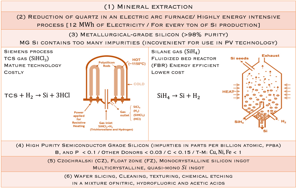
T.II.2: Schematic of Siemens ( batch process) and fluidized bed (FBR, continuous process) reactors
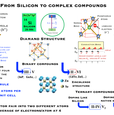
Starting with the group IV class of tetrahedrally bonded semiconductors we can go forward to binary and ternary compounds according to the Grimm-Sommerfeld rule, i.e. there must be an average of 4 valence atoms per atomic site
The chalcopyrite structure II−III−VI2 can be obtained by doubling the zinc-blende structure along the z-axis and filling the lattice sites. Thus II−III−VI2 can be envisioned as the ternary analogue of the binary ZnS
The ternary chalcopyrite compounds can be derived from the binary zinc blend (III-V ; II-VI) by a substitution a substitution (III→II-IV ; II→I-III) without violating the four electrons per lattice site rule
Theoretical study reveals a strong p-d hybridization in II−III−VI2 but not in II-IV-V2 compounds, which can leads to significant impact on optical properties and the band gap with is by the way direct
II−III−VI2 such as CuInS2, Cu(In,Ga)(X,Y)2 (X = S, Y=Se) are successfully used as absorber materials in thin film solar cells.
In the crystal structure of silicon (known as the diamond lattice structure), each atom is covalently bonded to four equivalently adjacent atoms. Silicon belong to the group IV class of tetrahedrally bonded semiconductor of the periodic table. The band gap of Silicon at room Temperature, is 1.12 eV
Intrinsic Silicon: undoped semiconductor: equal number of electrons and holes, and the carrier concentration at RT (300 K) is approximately:
N-type doping -
Phosphorus (P, group VA) introduced to Si lattice bring 5 "valence electrons" which form covalent bonds with 4 neighboring silicon atoms. The 5th electron is a free conduction electron charge.
Silicon became n-type and P is“ DONOR” doping
Before doping n = p (one electron lefts behid one hole),
After doping with group VA n = p + ND where ND are ionized donors
P-type doping -
Boron (B, group IIIA) with one fewer electron than silicon, leads to a "HOLE" in the shell and silicon became p-type
BORON is considered as an “ Acceptor” doping with three outer electrons
Before doping n = p (one electron lefts behid one hole)
After doing: p = n + NA where NA are ionized acceptors
From group IV into binary and ternary compounds
Source: S.M. Sze, Semiconductor Devices, Physics and Technology, John Wiley & Sons, Inc.

T.II.3: Schematic
REFERENCES -
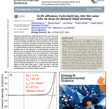
11.3% efficiency Cu (In, Ga)(S, Se)2 thin film solar cells via drop-on-demand inkjet printing, X. Lin, R. Klenk, L. Wang, T. Köhler, J. Albert, S. Fiechter, A. Ennaoui Energy & Environmental Science 9 (6) (2016) 2037-2043
Monolithically interconnected lamellar Cu (In, Ga) Se2 micro solar cells under full white light concentration, B. Reinhold, M. Schmid, D. Greiner, M. Schüle, D. Kieven, A. Ennaoui, Progress in Photovoltaics: Research and Applications 23 (12), (2015) pp 1929-1939
Cu2ZnSnS4 thin film solar cells from electroplated precursors: novel low-cost perspective, A. Ennaoui, M. Lux-Steiner, A. Weber, D. Abou-Ras, I. Kötschau, H-W. Schock, R. Schurr, A. Hölzing, S. Jost, R Hock, T. Voß, J. Schulze, A. Kirbs,Thin solid films 517 (7), (2009) 2511-2514
Buffer layers and transparent conducting oxides for chalcopyrite Cu (In,Ga)(S,Se)2 based thin film photovoltaics: present status and current developments, N. Naghavi, D. Abou‐Ras, N Allsop, Nicolas Barreau, S Bücheler, A Ennaoui, C‐H Fischer, C Guillen, D Hariskos, J Herrero, R Klenk, K Kushiya, D Lincot, R Menner, T Nakada, Charlotte Platzer‐Björkman, S Spiering, AN Tiwari, Tobias Törndahl, Progress in Photovoltaics: Research and Applications 18 (6), (2010) 411-433
Defect study of Cu2ZnSn(SxSe1-x)4 thin film absorbers using photoluminescence and modulated surface photovoltage spectroscopy, X. Lin, A. Ennaoui, S. Levcenko, T. Dittrich, J. Kavalakkatt, S. Kretzschmar, Applied Physics Letters 106 (1) (2016) 013903.
Highly‐efficient Cd‐free CuInS2 thin‐film solar cells and mini‐modules with Zn(S,O) buffer layers prepared by an alternative chemical bath process, A Ennaoui, M Bär, J Klaer, T Kropp, R Sáez‐Araoz, MC Lux‐Steiner, Progress in Photovoltaics: Research and Applications 14 (6), (2006) 499-511.
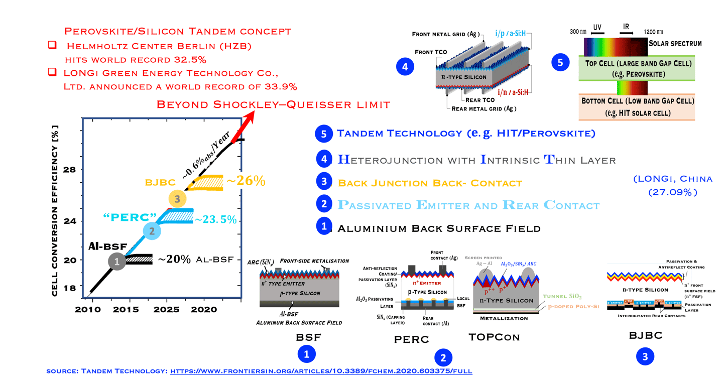
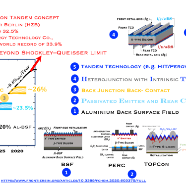
Historical and expected solar cell efficiency roadmap
Monocrystalline based silicon solar cells have improved in terme of efficiency over time due to the innovation in the manufacturing processes, and cell architecture. The objective of research working in the improvement of the efficiency is to approach the fundamental efficiency limit. W. Shockley and H. J. Queisser demonstrated the band gap dependent efficiency limit of solar cells based on detailed balance and hole–electron pairs ´s radiative recombination mechanisms. The maximum efficiency limit is closed to 30% for crystalline Si with an energy gap of 1.1 eV. As shown in (T.III.1), the first Silicon solar cell technology developed dominating the marked is the so called Al-BSF "Aluminum Back Surface Field" followed by PERC "Passivated Emitter and Rear Cells". Both are available in large-scale industrial PV production. Al-BSF is the first mature architecture that has reach a significant upscaling of ca. 450 GW per year. PERC solar cells, contain more innovation compared to Al-BSF, the innovation in PERC, comme from the fact that the full area Al-BSF is replaced by local dielectric aluminium oxide (AlOx) contact across the rear surface, such contact to the substrate is achieved by opening via laser ablation or wet chemistry. Such selected contact reduces rear-surface recombination and improved rear- surface reflectivity. Here are a few important steps for processing solar cells:
Wafer Cleaning, Etching, and Texturization
Phosphorous (P) diffusion (doping) with formation n+ emitter on p-type silicon by Thermal diffusion to create p-n+ junction
Passivation on front-side silicon nitride (SiNx) and anti-reflection coating (ARC)
Ag-finger screen printing contact on the front
Al-screen printing on the rear creates p+ region at the rear surface acts as a p-type dopant
Al-BSF cells suffer from recombination losses limiting the efficiency to 20% (see illustration)
PERC with reduced recombination centers on the back surface by passivating the dangling bonds in the dielectric And increasing light reflection on the back surface, leads to higher short circuit current density (JSC), and reduces the saturation current of solar cells (J0)
PERC showed an efficiency increase of approximately 4% in absolute value, with an optimum voltage of 708 mV, the evolution of the yield which reaches a plateau of approximately 23% is shown in the above diagram. Another advantage PERC cells can be made bifacial
Sources: W. Shockley, H. J. Queisser, J. Appl. Phys. 1961, 32, 510 // Matthew Wright, et al. Energy Environ. Sci., 2023, 16, 4164–4190 // International Technology Roadmap for Photovoltaics (ITRPV); Results 2023; Fifteenth Edition, May 2024 // Report 2024 on Trends in PV Applications 2024; International Energy Agency (IEA) // PV magazine information.
Passivation of the contacts was used by SunPower since the 2010s for its interdigitated back contact solar cells,
Further innovation known as TOPCon (short for Tunnel Oxide Passivated Contact), where a wide band-gap dielectric layer such as (SiOx), and a polycrystalline silicon layer create higher efficient (TOPCon is introduced by Feldmann et al. at Fraunhofer ISE in 2013). [F. Feldmann, et al. 28th Eur. PV Sol. Energy Conf. Exhib., Paris, September 2013]
An industrial version of TOPCon, known as industrial TOPCon (I-TOPCon), consists of improving p-PERC technology, since the two processes (PERC and TOPCon) are PERC cell, with only additional steps in the production line.
The TOPCon architecture deliver high efficiencies of approx. 25.0% in pilot and serial production at major cell manufacturers, with record efficiencies of over 26.0%.
As reported by "PV Magazine", The key issue of I-TOPCon is to achieve high conversion efficiency in mass production in order to compete with the state-of-the-art PERC cell in terms of system cost and levelized cost of electricity,”
TASK-III: Evolution of Silicon PV Technology from the perspective of technological innovation
Crystalline silicon (c-Si) solar module has dominated the PV market for several decades. The learning curve (T.I.2 ) shows that we are entering the “grid-parity” era of solar-generated electricity. Currently (2023), module shipments hit a record high of 502 GW, with cumulative installed PV capacity rising to around 1,610 GW throughout the world. We believe still important identify new design and manufacturing innovation, and to go trough the research portfolio and the impact of economies of scale.
sources: Task 1 Strategic PV Analysis and Outreach – 2023 Snapshot of Global PV Markets // Report IEA-PVPS T1-42: 2024
T.III.1: Evolution of silicon solar cell efficiency including the emerging next generation solar PV technologies toward carrier selective contacts, namely: Al-doped Back Surface Field (Al-BSF), Passivated Emitter and Rear Cells (PERC) , Tunnel oxide passivating contact (TOPCon), Crystalline Silicon heterojunction with Intrinsic layer HIT solar cells and Tandem structure c-Si (HIT) / Perovskite
(sources: M. Hermle, Fraunhofer ISE and webinar of Ivan Gordon (IMEC)
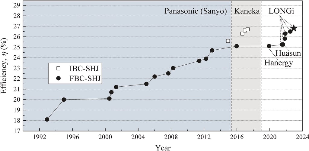
T.IV.1 - Certified record efficiency progression of SHJ solar cells starting with certified ‘HIT’ solar cell reported by Panasonic (Sanyo) in 1992 (not certified). LONGi and Huasun achieved a certified efficiency of 25.26% in June and July of 2021, respectively, while LONGi's cell having an area of 244.53 SQCM and Huasun's cell having an area of 274.5 SQCM respectively. Fig. as published by [Yifeng Zhao et al. Sol. Energy Mater. Sol. Cells 258 (2023) 112413]
Task IV - Exceeding the SQ limit: R&D on Perovskite/HIT Tandem solar cells
Combining multiple solar cells into a Tandem system, can capture more energy of the solar spectrum and convert sunlight into electricity more effectively. Tandem solar cell with Perovskite solar cell as top cell and HIT as bottom cell shows that more photons from solar spectrum can be collected and promising results exceeding the SQ limit in term of efficiency can be obtained. Other absorber such as CIGS absorber for the bottom cell can be also used
Silicon/Perovskite and Silicon/CIGS Tandems:
Perovskite solar cells started with a conversion efficiencies below 4% in 2009, followed by certified single-junction solar cell efficiency of 26.7% in 2024 and Tandem Si/perovskite solar cells have reach a an efficiency of 34.6%
Band gap Engineering and the development of high-quality interface passivation structures as well as the development of new electron transport films are the key issues for stable and high-efficiency solar cells and modules
LONGi Green Energy Technology Co., Ltd. reached new world record efficiency of 30.1% for silicon perovskite tandem solar cell (announced in Intersolar Europe in Munich, Germany on June 19, 2024 at the 2024). Their efficiency (30.1%) was certified in Germany at Fraunhofer Institute for Solar Energy (Fraunhofer ISE). LONGi announced a new world record of of 34.6% tandem solar cell efficiency at the 2024 SNEC EXPO in Shanghai
Monolithic perovskite/CIGS tandem solar cell with a certified power conversion efficiency (PCE) of 24.2% was obtained
sources: [NREL Best Research-Cell Efficiency Chart, https://www.nrel. gov/pv/cell-efficiency.html (accessed Jan 8, 2025)]. [“Highly Efficient and Stable” Perovskite Solar Cells: Hype Versus Reality, Prashant V. Kamat, ACS Energy Letters 2025 10 (2), 896-897]; [Marko Jost et al. Perovskite/CIGS Tandem Solar Cells: From Certified 24.2% toward 30% and Beyond, ACS Energy Lett. 2022, 7, 1298−1307]
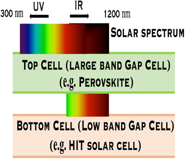

T.IV.1 - Top cell perovskite/Bottom cell either HIT (left) or CIGS (right): The perovskite layer is the top cell tuned to play the role of the large band gap and absorb the higher-energy from the solar spectrum. HIT silicon cell , or CIGS means Cu(In,Ga)(S,Se)2 absorber thin film demonstrated high efficiency
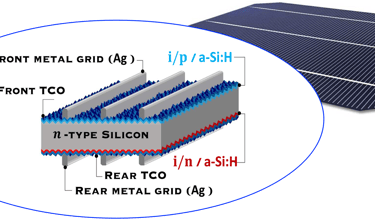
Silicon heterojunction with Intrinsic Thin Layer (HIT) as bottom cell: Prospect
Pioneered by Japanese electronics company Sanyo ca. 20 years ago, HIT cell architecture consists of the deposition of two thin amorphous silicon (a-Si) layers onto both sides of the c-Si wafer after wet chemical texturing and surface cleaning, [https://www.maysunsolar.com/what-is-hjt-technology-for-solar-modules/]
The first a-Si is intrinsic (i-a-SiH), an passivates defects present on the crystalline silicon surface (n-type, c-Si), and reduces the recombination of charge carriers at the interface, this enable to optimise several parameter of the solar cell such as open-circuit voltage (Voc = 750mV)
The second a-Si layer is doped and creates the p-n device junction with c-Si, then, a transparent conductive oxide layer (TCO), with excellent transparency and conductivity, and negligible parasitic absorption losses is deposited followed by the front metallization, mainly obtained by printing
Transparent Conducting Oxyde (TCO) deposited on both side makes the symmetrical HIT cell is suited to bifaciality (i.e. both sides of the panel can generate power using albedo) and exhibits an excellent temperature coefficient (-0.24%/°C) in the field making HIT more adapted for higher temperatures environment (like desert regions).
HIT is fabricated with fewer process steps compared to PERC and TOPCon cells
After the patents of Panasonic’s HIT technology expired (2010), several equipment suppliers and manufacturers start working with the technology, and providing equipment such as PECVD, PVD, vacuum sputtering equipment, and wet chemistry tools, which create a huge dynamic in PV market
There are several technical challenges at different part of HIT solar cell structure (right illustration) .
High quality c-Si/a-Si interface, this requires careful preparation of the substrate c-Si wafer (wet chemical texturing and surface cleaning)
Optimal passivation of a-Si/c-Si junctions
Uniformity of TCO layers
Sources: PV Magazine (Momentum builds for HJT, by Jonathan Gofford)
[https://www.pv-magazine.com/magazine-archive/momentum-builds-for-hjt/]
Illustration from [https://www.maysunsolar.com/what-is-hjt-technology-for-solar-modules/]

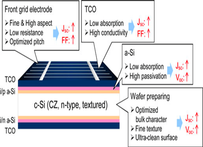
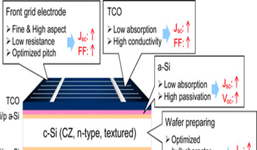
T.IV..2 - Bottom cell: Silicon heterojunction(SHJ) solar cells with intrinsic a-Si thin layer (i/p a-Si and i/n a-Si), and TCO are deposited from both side. The illustration (right) shows several optimisation opportunities to improve the performance of the device
Organic/Inorganic Perovskite as top cell: Prospect
Several thin films deposition techniques are available for processes Perovskite solar cell such as spin coating, drop casting, slot-die coating, inkjet printing
Conductive Transparent Oxides (TCO), which do not absorb in visible as well as materials known as electron transport layer (ETL), and hole transport layer (HTL) are the baseline for processing Perovskite devices
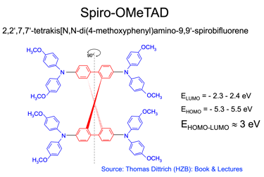
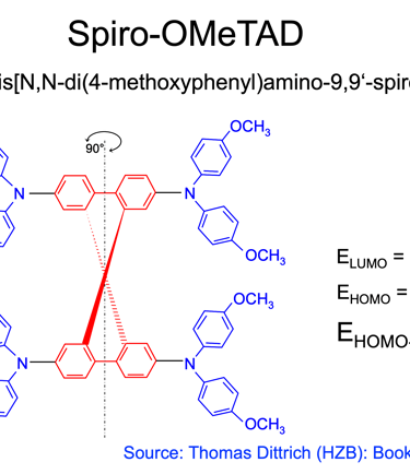
The most used materials for charge collection are Polymeric HTLs like Spiro MeOTAD and P3HT, and show stability at high temperatures, water resistant, and compatible with other materials for band alignment
Research and development is still ongoing to explore new effective charge transport materials (for electrons and holes) with specific properties such as environmentally friendly materials, cost-effective, scalable manufacturing, efficient charge transfer, and long-term stability
sources: https://www.maysunsolar.com // [Mikio Taguchi et al. PROGRESS IN PHOTOVOLTAICS: RESEARCH AND APPLICATIONS Prog. Photovolt: Res. Appl. 2005; 13:481–488]
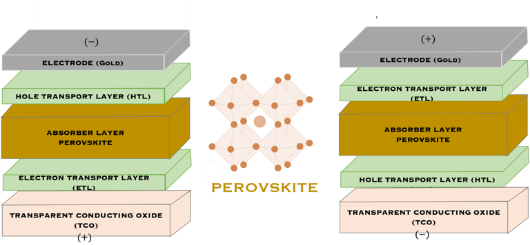
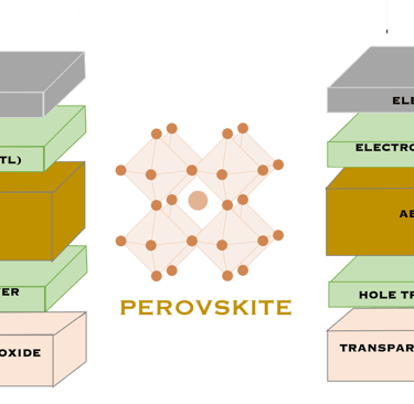
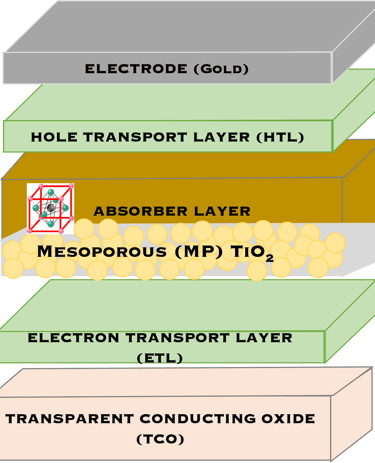
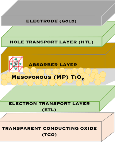
T.IV.3 - Top cell perovskite: Normal (LEFT) and inverted (RIGHT) structures, both contains perovskite layer (absorber), transparent electrodes, the only difference is the electron transport layers (ETL) and hole-transport layers (HTL) are inverted
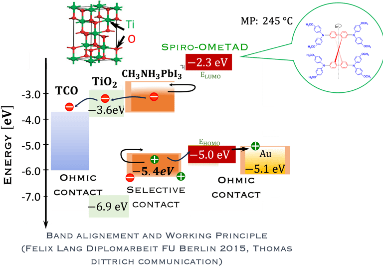
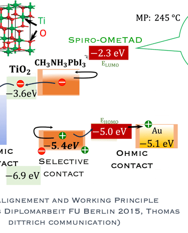
T.IV.4: Band diagram and energy levels of conventional Perovskite solar cell. Valence and conduction band of TiO2 ((ETL). Light harvesting Perovskite layer which placed between electron transporting layers (ETL) and organic Spiro OMeTAD layer (HTL). The electrons are transferred to ETL and holes move toward HTL. The conduction band energy of TiO2 is lower than the conduction band of Perovskite, thus, electrons are transferred from perovskite to the ETL and then to FTO. Meanwhile, holes move to the metal electrode easily because HOMO of HTL (Spiro OMeTAD) is higher than HOMO of Perovskite (CH3NH3PbI3)
Here are the most relevant information on material engineering to ensure efficient charge carrier transfer:
(1) Electron transporting layer (ETL)
(2) Hole transporting layer (HTL)
(3) Free electrons and holes (photo generated) are injected into (ETL) and (HTL) respectively
(4) Mesoporous Titanium Dioxide (anatase TiO2) is the traditional ETL used in High efficiency device
(5) Spiro-OMeTAD (HTL) is the most suitable holes transport layer used for high performance solar cell devices
(6) Fluorine-doped tin oxide (FTO) glass is used as electrodes
(7) Electrons are transferred to ETL and holes move toward HTL
(8) The conduction band energy of TiO2 is lower than the conduction band of Perovskite
(9) HOMO of HTL (Spiro OMeTAD) is higher than HOMO of Perovskite (CH3NH3PbI3)
(10) Electrons are easily transferred from perovskite to the ETL and then to FTO. Meanwhile, the holes move to the metal electrode
[source: Aschariya prathan et al. Scientific Report (2020), see also the book by Thomas Dittrich Materials concepts for solar cells and simple chemical methods for thin film deposition by Babasaheb R. Sankapal, Ahmed Ennaoui, Ram B. Gupta, and Chandrakant D. Lokhande ]
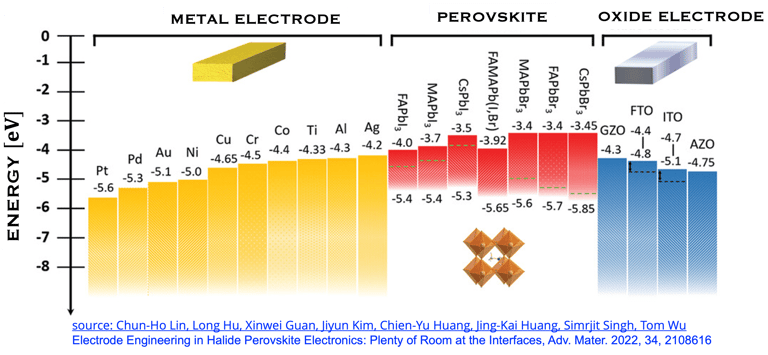
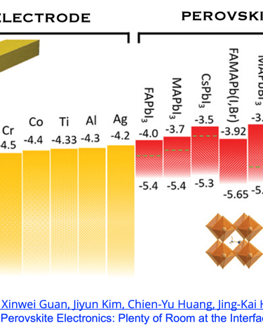
T.IV.5: Perovskites solar cells band gap, indicating the optimized energy level alignment with selected potential metals and oxides. The data help to choose suitable electrodes for perovskite contact electrodes, however, several mechanisms are associated with interfaces make the problem rather complexe. Figure and comments as published by Chun-Ho Lin et al. in Advanced Materials 2022, 34, 2108616,
Structures and Properties of Perovskite Family - baseline architecture of Perovskite solar cell - Energy levels alignement
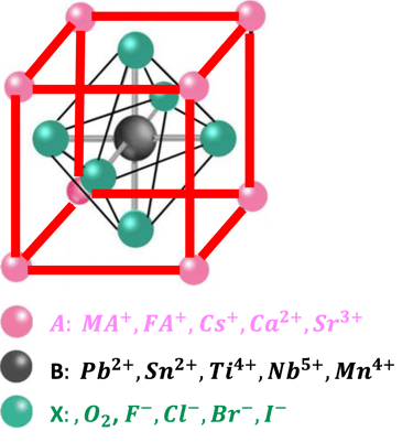
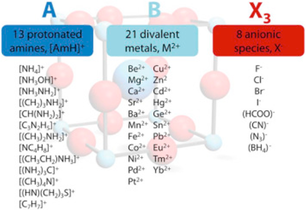
Perovskite is a class of materials with a crystal structure similar to the mineral perovskite, calcium titanium oxide (CaTiO₃).
The perovskite structure consists of a cubic unit cell, in which the cation “A” are located the corners of the cube, cation “B” in the center of the cell, and anion “X” at the edges (at midpoints)
The general formula ABX₃ is represented by the three-component “A” and “B” the cations of different sizes, and “X” an anion. This results in 3D networks BX6 octahedral units held together in place by large A-site cations such as the organic MA and FA, Cs, Ca, Sr, ...
The following “Goldschmidt Tolerance Factor (GTF)” for cation and anion radii has been used for predicting the most stable perovskites structure in the 3D perovskite system
A wide range of cations and anions can give a wide range of perovskite materials according to GTF
Goldschmidt Tolerance Factor (GTF) rule

RA., the effective ionic radius of the protonated amine A
Rx the ionic radius of the anion X,
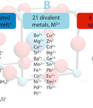
RB the ionic radius of the divalent metal ion B


sources: Chun-Ho Lin et al. Electrode Engineering in Halide Perovskite Electronics: Plenty of Room at the Interfaces, Advanced Materials 2022, 34, 2108616
O. Grånäs, et al. Establishing the limits of efficiency of perovskite solar cells from first principlesmodeling. Sci Rep 6, 36108 (2016)
G. Kieslich, et al. An extended Tolerance Factor approach for organic–inorganic perovskites, Chem. Sci., 6 (2015), pp. 3430-3433
Copper Indium Gallium Selenide CuInxGa1-x)Se2 (CIGS) is well adapted as bottom cell with Perovskite as top cell: Prospect
Several research works demonstrate that the well established thin films of polycrystalline copper indium gallium selenide CuInxGa1-x)Se2 solar cell is is well adapted and promising mandate to realize a tandem cell with Perovskite as top cell
Helmholtz-Zentrum Berlin (HZB) and Humboldt University Berlin have fabricated CIGS/Perovskite tandem solar cell with record efficiency of 24.6% certified by the Fraunhofer Institute for Solar Energy Systems
At HZB, monolithically integrated perovskite/CIGS tandem solar cell with a certified power conversion efficiency (PCE) of 24.2% is demonstrated
The tuning of the bandgap energies over a broad range can be realized for both materials: the bottom cell CuInxGa1-x)Se2 (CIGSSe) and the top cell Perovskite, through compositional engineering, thus there is plenty of room for optimisation
sources: Marko Jost et al. 21.6%-Efficient Monolithic Perovskite/Cu(In,Ga)Se2 Tandem Solar Cells with Thin Conformal Hole Transport Layers for Integration on Rough Bottom Cell Surfaces, ACS Energy Lett. 2019, 4, 583−590, Marko Jost et al. Perovskite/CIGS Tandem Solar Cells: From Certified 24.2% toward 30% and Beyond, ACS Energy Lett. 2022, 7, 1298−1307 // Martin Stolterfoht et al. How To Quantify the Efficiency Potential of Neat Perovskite Films: Perovskite Semiconductors with an Implied Efficiency Exceeding 28%, Adv. Mater. 2020, 32, 2000080 // Fan Fu et al, Monolithic Perovskite-Silicon Tandem Solar Cells: From the Lab to Fab, Adv. Mater. 2022, 34, 2106540
Both materials CIGS and Perovskite can be deposited on flexible substrates in a roll-to-roll process using e.g. inkjet printing, this open new applications such as "Building-Integrated Photovoltaics" (BIPV)
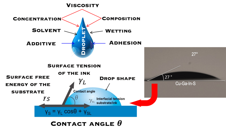
Inkjet printed CIGS is well adapted for Perovskite/CIGS tandem solar cell
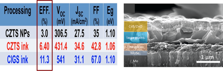
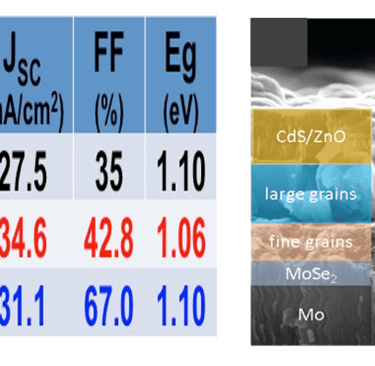
In 2015 we developed a techniques and processes for the deposition of CIGS absorbers and related solar cell (Project ATHLET), the objective is to reduce the price of the photovoltaic (PV) modules further. This project focus on the development of low cost processes and sustainable thin film materials to obtain cheaper, flexible photovoltaic solar cells with CIGS and CZTS (work developed during the PHD thesis of Xianzhong Lin (15 November 2013) from Guangdong, China
Both CIGS and CZTS absorbers have intrinsically p-type conductivity with a tunable direct band-gap
Solar cells with CIGS reached an efficiency of 23.35%, with absorbers fabricated via vacuum deposition methods.
Solution processing techniques, such as inkjet printing may reduce the fabrication cost of the absorbers and lower financial barriers to commercialization.
We developed a promising device efficiencies with 11% efficiency using formulated ink and ink jet-printing
Inkjet printed CIGS is well adapted for Perovskite/CIGS tandem solar cell
In 2015 we developed a techniques and processes for the deposition of CIGS absorbers and related solar cell.
REFERENCES -
11.3% efficiency Cu (In, Ga)(S, Se)2 thin film solar cells via drop-on-demand inkjet printing, X. Lin, R. Klenk, L. Wang, T. Köhler, J. Albert, S. Fiechter, A. Ennaoui Energy & Environmental Science 9 (6) (2016) 2037-2043
Monolithically interconnected lamellar Cu (In, Ga) Se2 micro solar cells under full white light concentration, B. Reinhold, M. Schmid, D. Greiner, M. Schüle, D. Kieven, A. Ennaoui, Progress in Photovoltaics: Research and Applications 23 (12), (2015) pp 1929-1939
Cu2ZnSnS4 thin film solar cells from electroplated precursors: novel low-cost perspective, A. Ennaoui, M. Lux-Steiner, A. Weber, D. Abou-Ras, I. Kötschau, H-W. Schock, R. Schurr, A. Hölzing, S. Jost, R Hock, T. Voß, J. Schulze, A. Kirbs,Thin solid films 517 (7), (2009) 2511-2514
Xianzhong Lin, Ahmed Ennaoui, et al. Cu2ZnSn(S, Se)4 thin film absorbers based on ZnS, SnS and Cu3SnS4 nanoparticle inks: Enhanced solar cells performance by using a two-step annealing process, Sol. Energy Mater. and Solar cells, Vol. 132, January 2015, Pages 221-229
Buffer layers and transparent conducting oxides for chalcopyrite Cu (In,Ga)(S,Se)2 based thin film photovoltaics: present status and current developments, N. Naghavi, D. Abou‐Ras, N Allsop, Nicolas Barreau, S Bücheler, A Ennaoui, C‐H Fischer, C Guillen, D Hariskos, J Herrero, R Klenk, K Kushiya, D Lincot, R Menner, T Nakada, Charlotte Platzer‐Björkman, S Spiering, AN Tiwari, Tobias Törndahl, Progress in Photovoltaics: Research and Applications 18 (6), (2010) 411-433
Defect study of Cu2ZnSn(SxSe1-x)4 thin film absorbers using photoluminescence and modulated surface photovoltage spectroscopy, X. Lin, A. Ennaoui, S. Levcenko, T. Dittrich, J. Kavalakkatt, S. Kretzschmar, Applied Physics Letters 106 (1) (2016) 013903.
Highly‐efficient Cd‐free CuInS2 thin‐film solar cells and mini‐modules with Zn(S,O) buffer layers prepared by an alternative chemical bath process, A Ennaoui, M Bär, J Klaer, T Kropp, R Sáez‐Araoz, MC Lux‐Steiner, Progress in Photovoltaics: Research and Applications 14 (6), (2006) 499-511.


The technique enable of generating microscale liquiddroplets by applying a pulse to a fluid ink
D-O-D inkjet generates droplets with volume undernanoliter with repeatability and reproducibility
Non-contact technique
Reduced fluid’s waste = Reduced C-footprint
A wide range of materials can be deposited (polymer, ceramic, semiconducting NPs ink)
Almost any object can be printed as long as precise digital data for it exist
High resolution Digital image
Direct image data deposition
Printing ink which solidifies after impact on a substrate
Producing Items just-in-time (manufacturing on Demand)
Combine Inkjet printing and laser technology
Reduced delivery time via decentralized production
D-O-D inkjet printing is not limited to solar PV manufacturing
Nano-Synthesis and Ink formulation
Hot injection bottom up synthesis is the most nano synthesis approach enable to obtain controlled monodispersed Naocrystals (NCs)
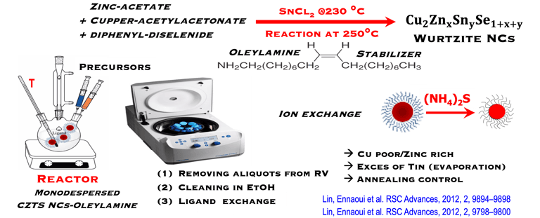
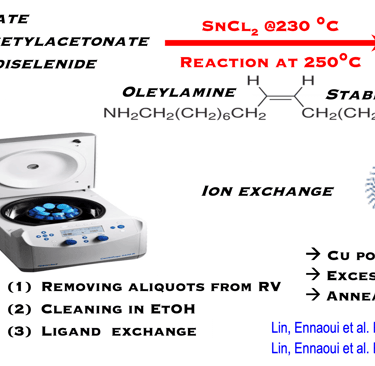
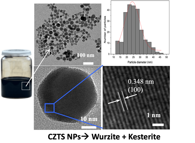
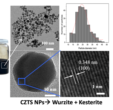
T.IV.7: Illustration for the synthesis of CZTS. Left: Hot injection preparation of CZTSSe NCs. The precursors used are copper oleate, zinc oleate and tin chloride as the cation precursors, including diphenyl diselenide and oleylamine. The preparation was carried out under nitrogen bubbling, heated to different temperatures. the mixture of SnCl2, oleic acid and oleylamine is injected with controlled temperature. The reaction solution was cooled down to room temperature. The NCs were precipitated with excess ethanol and were centrifuged at 6000 rpm. The resulting NCs were redispersed in toluene. Right: TEM image of as-synthesized nanoparticles and the corresponding size distribution histogram
[see more detail here: [Xianzhong Lin, Ahmed Ennaoui et al. RSC Advances, 2012, 2, 9894–9898]
T.IV.6: D-O-D inkjet printing tools
T.IV.8: Cross-sectional SEM images of a pre-heated Cu–In–Ga precursor (a) and of the best solar cell with an annealed CIGSSe thin film. Detailed data are explained in the full paper
[11.3% efficiency Cu (In, Ga)(S, Se)2 thin film solar cells via drop-on-demand inkjet printing, X. Lin, R. Klenk, L. Wang, T. Köhler, J. Albert, S. Fiechter, A. Ennaoui Energy & Environmental Science 9 (6) (2016) 2037-2043]
Task V: (Photo)electrochemical solar energy conversion: Artificial photosynthesis
INTRODUCTION - In previous webinars, Thomas Hannappel has focused on fundamental questions relating to energetic materials and the complex structures of semiconductors and their interfaces, which ensure the conversion of solar energy into chemical energy, in particular the production of hydrogen, or the reduction of Carbone dioxide into other forms of usefull fuels
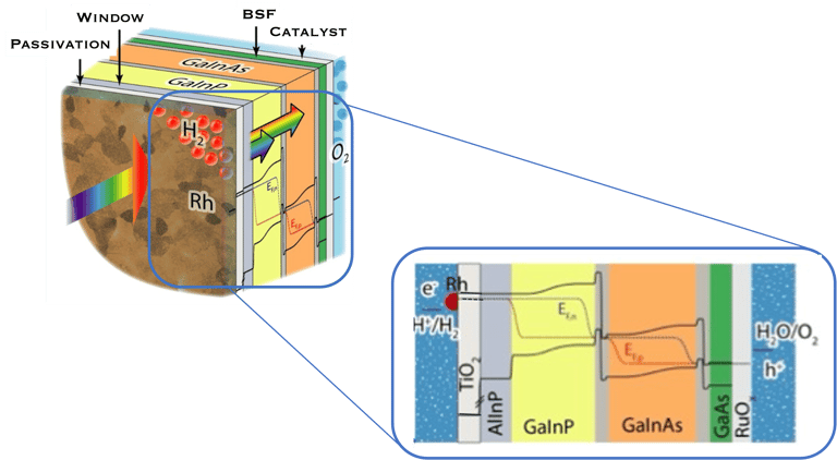
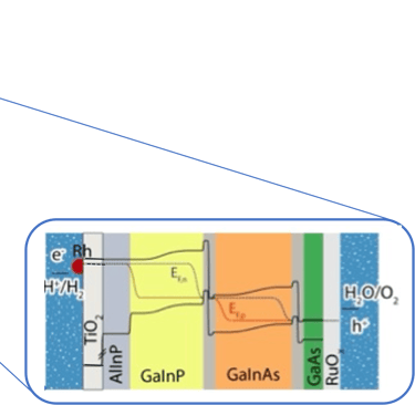
In such direct solar energy conversion well known as artificial photosynthesis, the sunlight absorption and electrochemical reactions occur in one single device (illustration below left). Thomas Hannappel, demonstrates a solar energy conversion into hydrogen with an efficiency of 19%, using tandem electrodes based on III-V compounds a very promising proof of concept
Illustration Rh/TiO2/Multijunction (AlInP/GaInP/GaInAs/GaAs)/RuOx tandem as record PEC device for unassisted water splitting.
sources: W.-H. Cheng, M. H. Richter, M. M. May, J. Ohlmann, D. Lackner, F. Dimroth, T. Hannappel, H. A. Atwater, H.-J. Lewerenz, ACS Energy Lett. 2018, 3, 1795-1800
Sol. RRL 2022, 6, 2200181//Sol. RRL 2024, 8, 2301047
ACS Energy Lett. 2020, 5, 470−476
Thesis (CALIFORNIA INSTITUTE OF TECHNOLOGY Pasadena, California)
Wen-Hui Cheng et al. "Integration of Multijunction Absorbers and Catalysts for Efficient Solar-Driven Artificial Leaf Structures: A Physical and Materials Science Perspective
Wen-Hui Cheng et al. CO2 Reduction to CO with 19% Efficiency in a Solar-Driven Gas Diffusion Electrode Flow Cell
Sisir Yalamanchili et al. High Broadband Light Transmission for Solar Fuels Production Using Dielectric Optical Waveguides in TiO2 Nanocone Arrays under Outdoor Solar Illumination
Sol. RRL 2024, 8, 2301047
ACS Energy Letters 3 (8), 1795-1800, (2018)
ACS Energy Lett. 2020, 5, 470−476
See also Thesis (Wen-Hui (Sophia) Cheng)
Towards High Solar to Fuel Efficiency: From Photonic Design, Interface Study, to Device Integration
Lesson learned from this work for high efficiency efficiency solar to Hydrogen
(1) High-performance and stable semiconductors photoanode (n-type materials) and photocathode (p-type materials)
(2) Optimal band gaps to collect solar spectrum
(3) Optimal Electronic properties and band alignment of all compounds
(4) Efficient photocatalytic materials for water splitting
(5) Stable Materials when exposed to agressive electrolyte (e.g. here TiO2)
(6) Dielectric structures for light tapping
(7) Challenges related to gas diffusion at the surface


Task VI: (Photo)electrochemical solar energy conversion: Power to X and Energy Transition
Energy transition and its challenges
As shown in the illustration (T-VI.1), the energy consumption and productions responsable of two-thirds of global emissions, and more than 80% of the global energy system is still based on fossil fuels [sources: S. Shiva Kumar and Hankwon Lim, An overview of water electrolysis technologies for green hydrogen production, in Energy Reports Volume 8, November 2022, Pages 13793-13813]
95% of the hydrogen production is comming from steamreforming of natural gas, (emitting 830 million tons/yearof CO2)
All sulphur compounds raw natural gas are converted to hydrogen sulphide, which is then removed
the processes of steam reforming of natural gas are wellunderstood and the technology is mature
Hydrogen is known as ‘Green hydrogen’’ when is produced from the conversion of CO2 free electricity, "Grey H2" when CO2 is released to the atmosphère and »blue H2" when CO2 is captured and stored
The consumption of natural gas is about 3.5 kg per kg of hydrogen produced, and the consumption of water is about 1.9 kg per kg of hydrogen production
Water electrolysis is the sustainable way to prevent 830 million tonnes of CO2 from entering the atmosphere every year
The implementation of sustainable energy system based on renewable energy become a must to build energy systems of tomorrow
Challenges: political inerties, Technical barriers, Societal challenges that require infrastructure upgrades, knowledge and awareness
Green hydrogen technology is the key to tackling the complexity of the problem, to finding an alternative to industries based on fossil fuels and natural gas
Green hydrogen enable the production of various synthetic fuels like green methane, methanol, or ammonia through Power-to-X processes
There are two way for ‘‘Green hydrogen’’ production, that commonly refers to hydrogen gas produced solely with renewable energy (figure T.VI.2)
Indirect production of ‘‘Green hydrogen’’ or Photovoltaic-coupled electrolysis.
Laboratory scale Solar-to-Hydrogen (STH) efficiencies over 30% was demonstrated by coupling two polymer electrolyte membrane electrolyzers in series with one InGaP/GaAs/GaInNAsSb triple-junction solar cell. Sun light hits the triple-junction device to produce the photovoltage for water splitting
Labelled indirect because the light is absorbed by a PV panel to provide power input into the electrolyzer, the technology is already mature up to the multi-megawatt scale
source: J. Jia, et al., Solar water splitting by photovoltaic- electrolysis with a solar-to-hydrogen efficiency over 30%, Nat. Commun., 2016, 7, 1–6
Direct production of ‘‘Green hydrogen’’ or Photoelectrochemical (PEC) water splitting
Laboratory-scale devices have been demonstrated with solar-to-hydrogen (STH) efficiencies of 19% Solar to Hydrogen (STH) for PEC cell
source: W. H. Cheng, et al., Monolithic Photoelectrochemical Device for Direct Water Splitting with 19% Efficiency, ACS Energy Lett., 2018, 3, 1795–1800
This concept is labelled direct because the light is absorbed directly by a semiconducting electrode in a PEC splitting water into oxygen and hydrogen. This system still in the level of proof of concept, and the scalability is not yet established
Lecture from source: Brian Tam et al. Energy Environ. Sci., 2024, 17, 1677–1694 // The Royal Society of Chemistry 2024
T.VI.1: Hydrogen production and consumption adapted from the paper of S. Shiva Kumar and Hankwon Lim, An overview of water electrolysis technologies for green hydrogen production, in Energy Reports Volume 8, November 2022, Pages 13793-13813
T.VI.2: compares the two concept for water splitting. Indirect water decomposition (Right), where PV panel is coupled with alcaline electrolyzer or polymer electrolyte membrane electrolyser (center). Direct water decomposition (Left) where the electrodes in a photo-electrochemical (PEC) is directly illuminated
Task VII: (Photo)electrochemical solar energy conversion: Learning from the nature
T.VII.4: - Photoelectrochemical (PEC) tandem arrangement, which combines a photoanode (n-type semiconductor) and a photocathode (p-type semiconductor) under illumination. (Left) - schematic of a system for the oxydation of water and reduction of hydrogen protons as well as the conversion (reduction) of Carbone dioxide (CO2) into useful chemical products [source: Wen-Hui Cheng et al. Hydrogen from Sunlight and Water: A Side- by-Side Comparison between Photoelectrochemical and Solar, ACS Energy Lett. 2021, 6, 3096−3113]
Inspired from the membrane structures of the leaves, it is important and informative to learn from the nature how plantes have approached the problem of solar energy conversion,
Comparing direct solar energy conversion in the structure of semiconductors electrodes under illumination in a PEC with the photosynthesis systems
Keeping in mind that, the structures in the plants for converting sunlight are 10,000 times thinner than the structure of semiconductors
What are the challenges of water splitting into green hydrogen or the electrochemical reduction of carbone dioxide
Several processes that occurs in the plant can be reproduced in the lab
The processes of photon absorption where the light energy from the sun is absorbed by the photoelectrode
Electron-hole generation: The absorbed light creates electron-hole pairs in the semiconductor
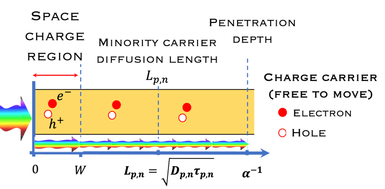
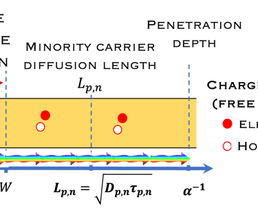
The thickness of the semiconductor electrodes should be larger than the minority carrier diffusion length
Water oxidation: The photoinduced holes on the photoanode surface oxidize water to form hydrogen and oxygen
Electron migration: The electrons move towards the cathode through an ohmic contact
Hydrogen production: The electrons reduce hydrogen protons at the cathode to produce hydrogen gas
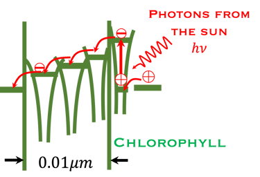
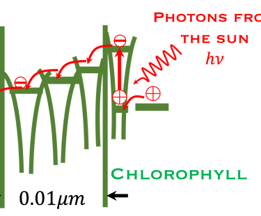
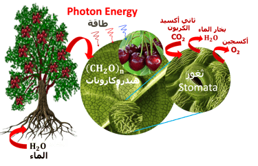

T.VII.3 Left-top: Light induced excitation and electron injection into a membrane in chlorophyll molecules. Left-bottom illustration the processes involved in both photosynthesis and artificial photosynthesis upon the light absorption: Right: simplified diagram of carbon dioxide capture by the plant including water absorption of sunlight, CO2 fixation to produce glucose and release of O2 in the atmosphere
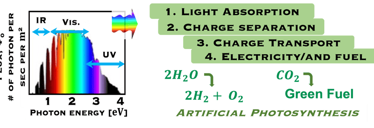
Comparing Natural and Artificial photosynthesis, four steps are shown (Right illustration):
The main processes involved for the production of electricity and usefull fuels are:
(I) Light is absorbed; (2) Charge are separated ; (3) Charges are transported to the surface and (4) consumed in electrochemical reaction to produce useful fuels
(II) In natural photosynthesis, green plants is maintaining the equilibrium of global carbon cycle by recycling the CO2 from respiration into biomass
(III) Water is pumped from the soil by roots to the leaves through transpiration via stomata, which open and close during gas exchanges with the environment
(IV) Carbone dioxide and water are reduced to glucose and oxidized to molecular oxygen respectively
(V) Electron transfer and reduction of CO2 in photosynthesis involves multi-steps reactions facilitated by enzymes or bio-catalysts (see T.VII.3 below)
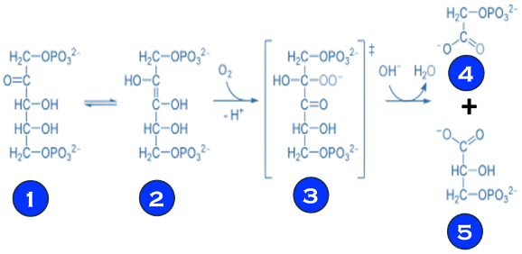


T.VII.3: RuBisCO: ribulose bisphosphate carboxylase/oxygenase is a key enzyme involved in the biological fixation of CO2
Sources: Madalena Gr´ acio et al. Food Chemistry 419 (2023) 135993, RuBisCO as a protein source for potential food applications https://en.wikipedia.org/wiki/RuBisCO // https://bioprinciples.biosci.gatech.edu/10-c4-plants/ // https://www.ncbi.nlm.nih.gov/pmc/articles/PMC3895110/
The first prototypes of (photo)electrochemical energy harvesting for solar to Hydrogen conversion was demonstrated in 1972 using TiO2, with efficiency of 2.2% because the anode used was a large band gap TiO2 rutile, which is absorbing in the UV region.
The state of the art with III–V semiconductors have reached a proof of concept of 19% efficiency for monolithic device structure
W. H. Cheng, et al., Monolithic Photoelectrochemical Device for Direct Water Splitting with 19% Efficiency, ACS Energy Lett., 2018, 3, 1795–1800
cited by Brian Tam et al, in an article entitled "Comparing the net-energy balance of standalone photovoltaic-coupled electrolysis and photoelectrochemical hydrogen production", Energy Environ. Sci., 2024, 17, 1677–1694
Regarding PEC solar harvesting systems for direct reduction of CO2 into energetic compounds(methane, ethane, and ethanol,...), the challenging issue is to find efficient catalysts
Photoelectrochemical reduction of CO2 into energetic compounds (methane, ethane, and ethanol,...) is a promising carbone dioxide recycling technique,
Artificial photosynthesis for CO2 reduction is inspired from natural photosynthesis in green plants using solar light
Various semiconductors act as an excellent photo-anode with optimal band gap and favorable energy band edge position for water splitting and CO2 reduction Nevertheless, the thermodynamic CO2 reduction involve multiple-electron products (T.VII.5) and requires selected catalysts
Need of favorable conditions fro both water splitting and CO2 reduction
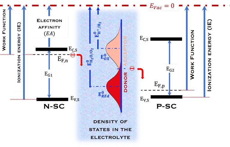
The photo-anode (N-type semiconductor) and the photocathode (P-type semiconductor), suitably selected with favorable electronic properties (band gap, electronic affinity, doping, work function of the metal, position of the valence and conduction band energies)
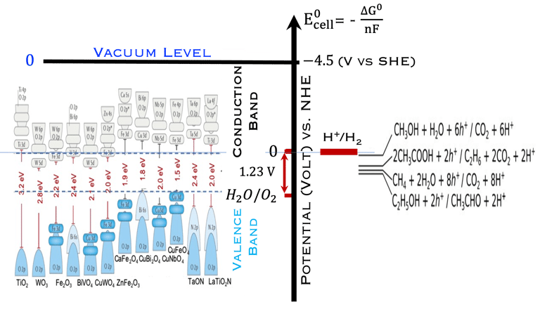
The position of potentials redox for oxidation and reduction including the position of Ev,s and Ec,s are as follow:
Anode: Ev,s < oxidation potential of water
Cathode Ec,s > reduction potential of hydrogen protons
The band gap should be large enough to absorb large amount of the sun spectrum
For efficient hydrogen production: The two semiconductor to absorb enough photons from Incident sunlight with photon energies E = 𝒉𝒄/𝝀) > Band gap
Catalytic sites on the surface of the anode and the cathode are required for selecting and accelerating the electrochemical reactions
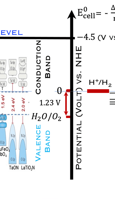
T.VII.5: (Right)- N-type and P-type semiconductor with the most important physical properties for selecting PEC electrodes. (Left)- The energy band diagram of several semiconductors showing the band edge positions in contact with the aqueous electrolyte (pH = 0) relative to SHE and the position of the redox system for water splitting at this pH. The energy gap between the valence and conduction bands which determines the potential of the materials to absorb sunlight and the composition of the valence band can be determined respectively from optical and XPS-UPS measurements. A task will be addressed for these issues including the calculation of flat band potential using electrical measurements of the capacitance of the space charge region the capacitance of the space charge region
Task VIII: Undestanding Electrochemical energy conversion from thermodynamic point of view
(PEM Electrolyser and and Fuel Cell PEM)
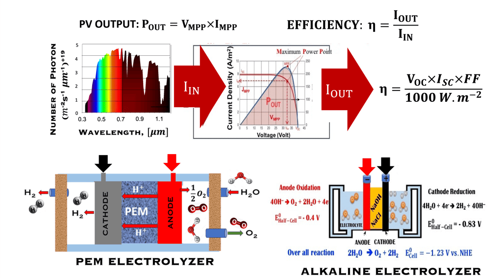
ΔG = ΔH–TΔS
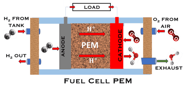
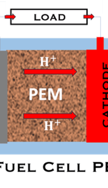
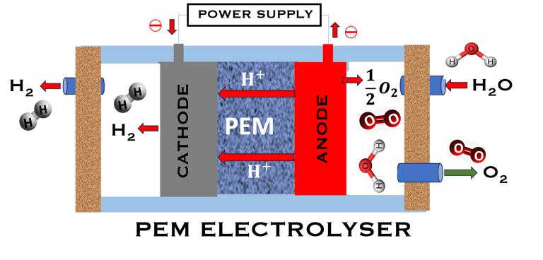
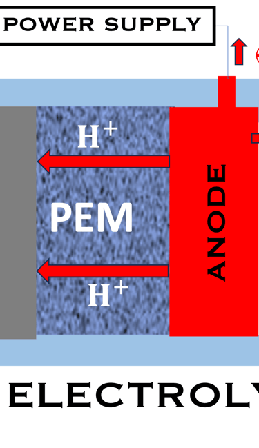
T.VIII.1a: (Left) - Proton Exchange Membrane fuel cells: (1) Hydrogen, from tank reacts at the anode (coated with catalysts) , where the oxidation takes place and releases electrons. (2) at the cathode (coated with catalyst), Oxygen from air is consumed and the reduction takes place. (3) electrons go through the external circuit, generating electricity in the form of direct current (DC) (4) protons migrate to the cathode, and combine with oxygen and the electrons producing water and heat. (5) a selected membrane allow only the protons to pass from the anode side to the cathode side. (Right) - T.VIII.1b: PEM electrolyser: (1) Water decompose at the anode into oxygen and positively charged hydrogen ions, (2) Hydrogen ions selectively move across the PEM to the cathode, while The electrons electrons flow through the external circuit. Hydrogen ions react with electrons to form hydrogen gas at the cathode,
Water is decomposed into O2 and H2 (Fuel)
O2 and H2 (Fuel) are combined and current (DC) is produced
FUEL CELL PEM
ΔG is the difference between the energy produced in an electrochemical process, ΔH, and the energy lost to the surroundings, TΔS
In an electrochemical cell working reversibly at (T and p), ΔG the net work is equal to the electrical work
In a fuel cell, the electrochemical reaction between hydrogen and oxygen is an exothermic reaction that produces electricity and heat
The enthalpy of formation ∆H = -285.84 kJ per mole, is the higher heating value provided from the combustion of hydrogen (H2 + 1/2 O2 → H2O + Energy)
The Gibbs free energy for the reaction ( - 237.2 kJ per mole ) represents the maximum electricity produced by a fuel cell
∆H can be divided into thermal energy, a entropy ∆S kJ per mol per K, multiplied by operational absolute temperature T, and useful work called Gibbs free energy ∆G kJ per mol, extracted as electrical energy: ∆G = ∆H + T∆S = - Q [coulombs] x E [V]
Q = number of electrons’ moles n multiplied by electric charge of one mole of electrons known as Faraday F = 96,485 coulombs per mole (C/mol)
Then ∆G defined as follow: ∆G= - n.F.E
he combustion of hydrogen is exothermic, thus ∆G, ∆H, and ∆S are negative
The potential given by the fuel cell is then: E = - ∆G/nF = - (∆H - T∆S) /nF
PEM ELECTROLYZER
The reaction is in the opposite way, and the water is decomposed into hydrogen and oxygen through an endothermic reaction: H2O + Energy → H2 + 1/2 O2
Here ∆G, ∆H, ∆S are positive as they must be supplied as a voltage applied to the electrolyzer: E = ∆G/nF
Positive value of Gibbs Free Energy (ΔG > 0) means non-spontaneity, e.g. water dissociation requires a minimum of free energy
ΔG is the difference between the energy produced by the process, ΔH, and the energy lost to the surroundings, TΔS
Negative change in Gibbs Free Energy (ΔG < 0) means that a reaction can occur without external energy input,
Positive value of Gibbs Free Energy (ΔG > 0) signifies non-spontaneity, e.g. water dissociation is non-spontaneous and requires a minimum of free energy
Electrochemical water splitting requires the following overall cathodic and anodic half-reactions (in acidic medium)
Standard conditions (T , p)
∆H°(T,p) = ∆G°(T,p) +∆Q°(T,p)
∆Q°(T,p) = T ΔS°(T,p) and ∆G°(T,p) = nFUcell
Ucell= EA – EC = difference of electrode potentials at the anode and cathode, respectively
The entropy change ΔS°(T,p) associated with the decomposition reaction of one mole of H2O can be calculated from the elementary entropy of each constituents:
ΔS°(T,p) = S(H2 ) + 0.5 x S(O2) – S(H2O)
ΔS°(298K, 1 bar) = 130.7 + 0.5 x 205.1 - 69.9 = 163.2 J per mole per Kelvin
ΔQ°(298, 1 bar) = T ΔS°(298K, 1 bar) = 298.15 x 163.2 = 48.6 kJ per mole
∆H°(298K, 1 bar) = ΔG°(298K, 1 bar) + ΔQ°(298K, 1 bar) = 237.2 + 48.6 = 285.8 kJ per mole

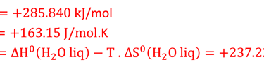
The theoretical minimum of electrical energy input (standard Gibbs free energy) required to dissociate water into hydrogen and oxygen at the standard conditions (T = 25 °C, p = 1 atm) is: ∆G° = - n . F . ∆E° = +237 kJ/mol of hydrogen or ∆E° = ∆G°(T,p)/nF = 1.23 V per electron
The number of electron transferred for one hydrogen mole is n = 2 and F ≈ 96485 C per mole : Faraday constant (product of the elementary electric charge by the Avogadro number).
The change in Gibbs free energy ∆G° = +237 kJ per mole of H2O corresponds to 1.23 eV per electron, in another word, the potential overall thermodynamic barrier for a water splitting reaction is 1.23 V.
When considering the total energy ∆H° = +285.840 kJ per mole of H2O, the value is 1.48V. The thermal energy is 48.7 kilojoules per mole is the heat released by the reaction
From the free energy equation: ∆G° = ∆H°–T∆S°, we conclude if ΔG is positive, then TΔS must be negative, which means that ΔS is negative. Therefore, the splitting of water into oxygen and hydrogen requires an energy supply, such as electricity (case of Electrolyzer) or light (case of photo-electrochemical cell (PEC)
T.VIII.1b: Simplified schematics of Coupling water alkaline electrolyzer (including PEM electrolyzer ) and photovoltaic (PV) solar technology, the schamatic shows the output production of PV under one sun. There are many challenges, such as: economies of scale in manufacturing, coupling and conversion) efficiency to reduce costs of hydrogen production, and increasing the lifetime and reliability of the systems to reach 20 to 30 years. source: Dr. Sonya Calnan (HZB), FVEE • Themen 2021, Wasserstoff-Erzeugung • Directly Coupled Photovoltaic Driven Water Electrolysis


Task IX: Photoelectrochemical Cells for water splitting
Subject covered
Starting point: bref description of a Photo-electrochemical cell
I - Semiconductors backgrounds
Intrinsic semiconductor, Doping levels, N-type and P-type semiconductor
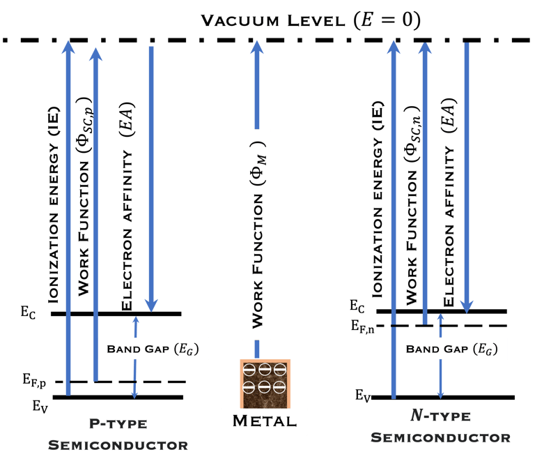
Vacuum energy level (Evac)
Conduction and valence band edge energy (Ec and Ev) , Fermi energy EF (or electrochemical potential)
Energy gap (EG), electron affinity (EA). onization energy (IE), work function (Φ)
Fermi–Dirac equation, and approximation of Maxwell-Boltzmann equation
II - Semiconductor–Inert Electrolyte Junction and Potential and Charge Distribution
Energy scale of Redox Electrolyte and energy levels of the oxidized and reduced species
Space charge region, band bending, and flat band potential
Semiconductor/Electrolyte in the dark and under illumination
Occupation of electrons and holes, excess carriers and Quasi Fermi Level, photoVoltage
III - (Photo) -Electrochemical measurements
Current–voltage plot in the dark and under illumination
Action spectra and External Quantum efficiency (EQE) measurements
Space charge capacitance, and Mott–Schottky equation
Evaluation of Solar to hydrogen efficiency
Starting point: bref description of a Photo-electrochemical cell
Below (T.IX.1), we represent a Photo-Electro-Chemical Cell (PEC) with consists of two electrodes: N-type semiconductor and P-type semiconductor in contact with an aqueous electrolyte
When the two semiconductor are placed in contact with an the electrolyte, electric current initially flows across the junction until electronic equilibrium is reached,
This means the Fermi level of N-type reach is aligned with redox energy level of the electrolyte meanwhile the Fermi level of P-type reach is aligned with redox energy level of the electrolyte
T.IX.1a: (Right) - Schematic showing the energy levels at the interface between a p-type semiconductor before contact awith the electrolyte. Because of the difference in the contact potentials, the electron flow from the electrolyte to the P-type semiconductor until the alignement of the fermi levels. (Left) - Schematic showing the energy levels at the interface between an n-type semiconductor before contact with an electrolyte, the difference in the contact potentials is the opposite and the electron flow from the N-type semiconductor to the electrolyte. The absolute scale (Vacuum level) and most relevant physical parameters are shown versus Vacuum Evac = 0
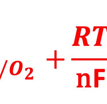
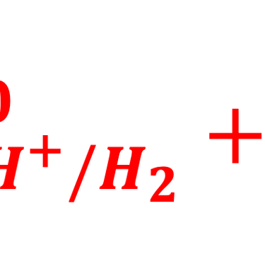
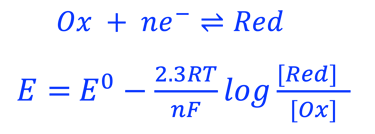
A electron in the redox couple in the electrolyte is represented by its electrochemical potential (called also Fermi level one electron redox-couple) given by Nernst equation.


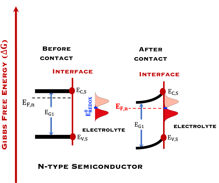
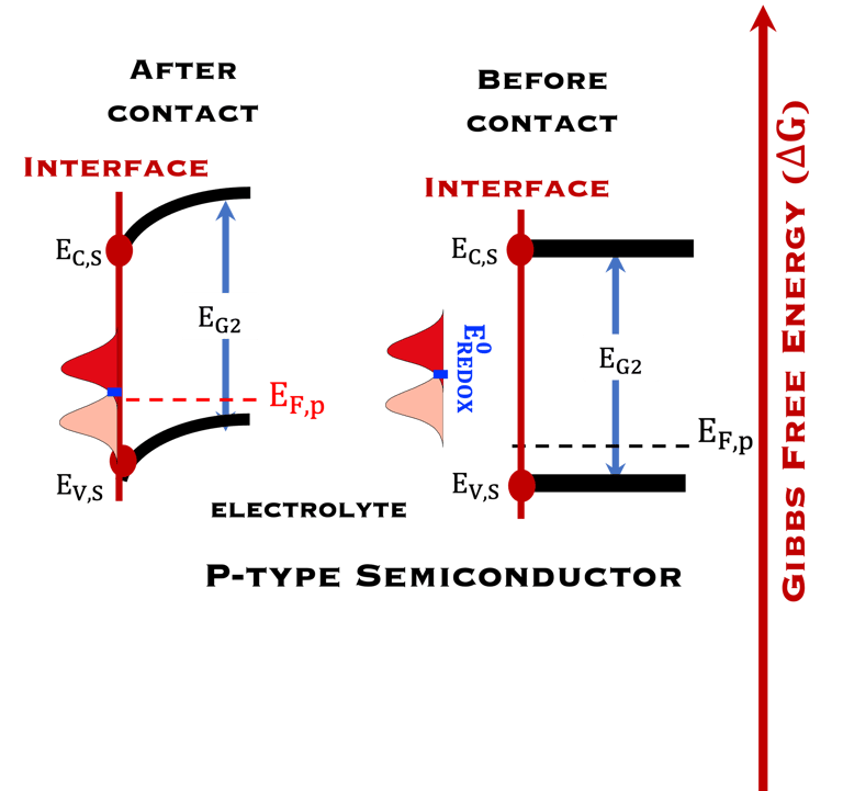
T.IX.1c: (Right) - Schematic comparing N-type and P-type semiconductors before and after contact with an electrolyte. The electrons transfer from the n-type semiconductor to the solution and from the solution to the p-type semiconductor creates a depletion layer in both semiconductors. The N-type semiconductor becames the anode positively charged, and the P-type semiconductor is the cathode negatively charged. The two phases solid/liquid are in equilibrium, the Fermi levels are aligned, and the charges at the interface balance each other (for a N-type semiconductor, the compensating charges are negatives). The energy bands of the semiconductor bend up for N-Type and down for P-type (for a P-type semiconductor, the compensating charges are positives ). A Schottky barrier is created with a space charge (Qsc) and a charge capacitance
In the next task on "measurements and techniques" we will describe the method for Mott-Schottky plot measurements and describe the capacitance of the interface
Providing some approximations, we can demonstrate the following equation (given here for N-type electrode)


Csc is the space charge capacitance, ε is the dielectric constant, ε0 is the permittivity of free space, A is the area of the electrode, e is the electronic charge, ND is the majority carrier concentration, V is the applied electrochemical potential, EFB is the flat band potential, kB is the Boltzmann constant, and T is the absolute temperature
We can determine the flat band potential at the interface semiconductor/electrolyte with the x-axis intercept of a Mott–Schottky plot and the slope can be used to determine the doping (donor or acceptor) concentration of semiconductor electrodes
The Fermi energy can then be calculated according to:
We describe below a PhotoElectroChemical cell (PEC) with N‐type semiconductor as photoanode and P‐type semiconductor as photocathode immersed in an aqueous electrolyte solution
The two electrodes are illuminated with photon energy E = 𝒉𝒄/( 𝝀) exceeding that of the band gap generate electron–hole pairs
The light penetrates the bulk of the semiconductor electrodes to varying depths depending on the wavelength 𝝀 of the light
The absorption coefficient determines how far light penetrates
Electron–hole pairs are photogenerated moved from the valence bande to the conduction band
The excess of electrons and holes generates a photo-Voltage
The electric field present in the space charge region (SCR) inside the semiconductor electrodes drives the electrons into the external circuit for the N-type photoanode and the holes move into the electrolyte solutions
The opposite electrical field in the P-type cathode drives the holes into the bulk of semiconductor and moves the electrons to the surface;
The electrochemical reactions take place at the surface of both electrodes:
At the photoanode water is oxidized into hydrogen proton, this requires Evs lies below O2/H2O (more positive potential than O2/H2O potential)
Electrons move trough the external circuit and reach the cathode with an electrochemical potential sufficiently negative (i.e., close enough to vacuum level Evac = 0) to reduction hydrogen protons
Solid state physic gives the edge of the conduction band and valence band levels of a semiconductor according to the values of electron affinity (EA) and ionization energy (IE), however a number of factors such as the surface termination and surface electronic states (dangling bond)
Such processes require favorable positions of the band edges (Ev,s for the N-type) and Ec,s for P-type) with the value of the generated photoVoltage VPH > 1.23 V enable
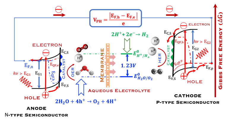
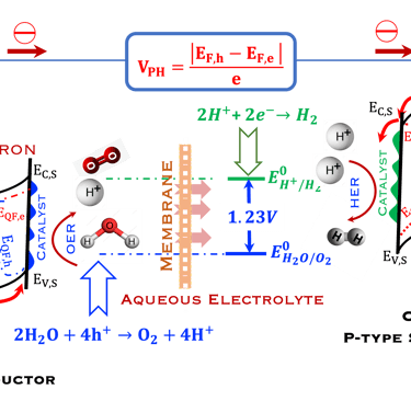
T.IX.2a: Schematic illustration of PEC with two electrodes consisting of a photoanode and a photocathode. The dashed lines represent quasi Fermi levels under illumination for N-type and P-type electrodes. The maximum generated photovoltage VPH is indicated
Absorption of light in a semiconductor. The space charge region, penetration depth, and the minority carrier diffusion length are indicated
Sources: K. Gelderman et al. Journal of Chemical Education, Vol. 84, (2007) 685-688
A. Ennaoui, et al. Iron disulfide for solar energy conversion, Solar Energy Materials and Solar Cells 29 (1993) 289-370
Wilson A. Smith et al. Energy Environ. Sci., 2015,8, 2851-2862
Ennaoui, A. Solar Energy Materials 14(6), (1986)pp. 461-474
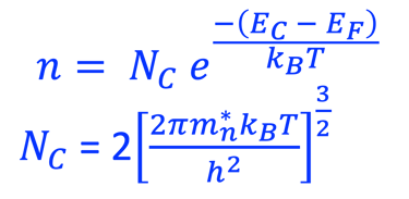
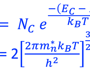
For N-type semiconductor:
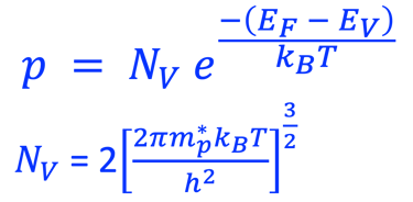
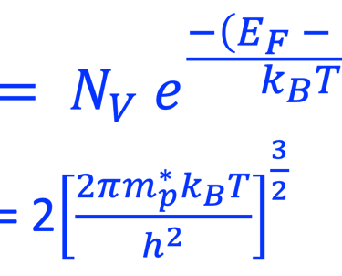
For P-type semiconductor:
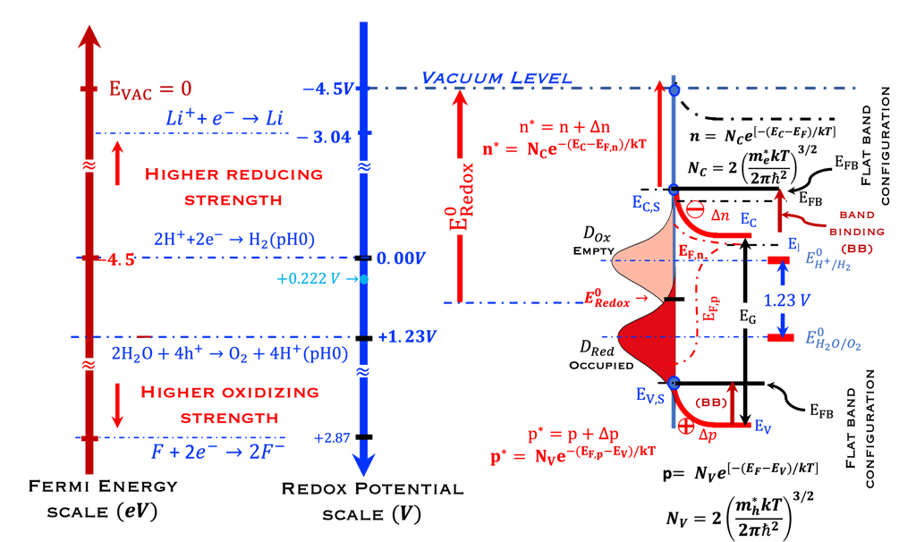
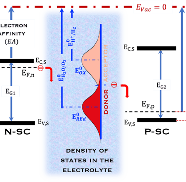
We ask the graduate students and visitors of this sciences & education webpage of Virtual Learning University to look at the diagram below:
Redox Potential Scale used by electrochemists based on redox potential
Fermi Energy Scale used by solid-state physicists based on vacuum level as a reference
Distribution of the occupied states in the electrolyte
Electrochemical reaction for water splitting in acidic solution, (0 V and 1.23 V pH 0)
Compared with the higher oxidation (fluorine) and higher reduction (lithium)
N-type semiconductor at Flat Band Potential position
Concept of the energy level of the oxidized (empty) and reduced (full) species,
Quasi-Fermi level of electrons and holes (EFn, EFn) and photovoltage (EFn - EFn)/e
Task X: Measurements and Techniques in Photoelectrochemistry
This task concerns the Electrochemical techniques and the standard operating procedures for testing semiconductor electrodes in a PEC:
The Potentiostat/Galnostat:
Potentiostat: Apply a controlled voltage range and measuring the current produced for specific redox reactions at the cathode and anode
measurement of I-V characteristics and the photocurrent onset potential for different photo-electrochemical reactions
Galnostat: Inject a controlled current range and measuring the current produced for specific redox reactions at the cathode and anode
Set-up for the Mott-Schottky plot analysis and potential across the Helmholtz layer
Determine the flatband potential: the position of the Fermi level of the semiconductor with respect to the potential of the reference electrode
Photo-electrochemical parameters of PEC cell to meets the best performance
Determine the spectral response (SR) and External quantum efficiency (EQE)
Determine Friday Efficiency (FE) and Solar to Hydrogen (STH) Efficiency
Discuss the conditions to be to be addressed to select reliable photo-electrode materials: Effective photo-induced charge carriers, Low over-potential
Large solar spectrum harvesting, High stability and long-term operation, Low cost and non toxic alternative materials
(Right) - comparison of three PEC Top made from glass, bottom one compartiment and two compartiment PEC
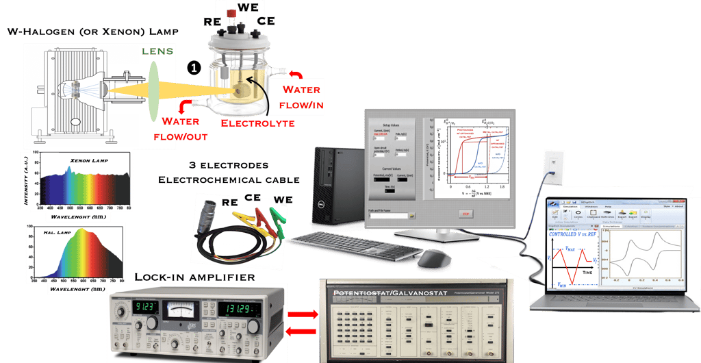
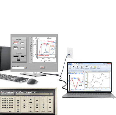
T.X.1a: (Left) - Experimental set up for cyclic voltammetry and Electrochemical impedance spectroscopy, it consists of (1) three electrode PEC with a Ag/AgCle reference electrode, (2) EG&G for potentiostatic I(V) and Galvanostatic V(I) measurements (EG&G is coupled with a lock-in amplifier for impedance (capacitance) measurements , (3) W-Hal or Xe lamps to simulate solar radiation (the spectra of W-Hal and Xe are shown); (4) The system woks well with LabVIEW programming software package based system for electrochemical control and measurements.


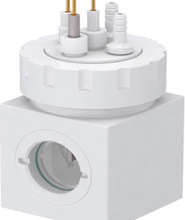
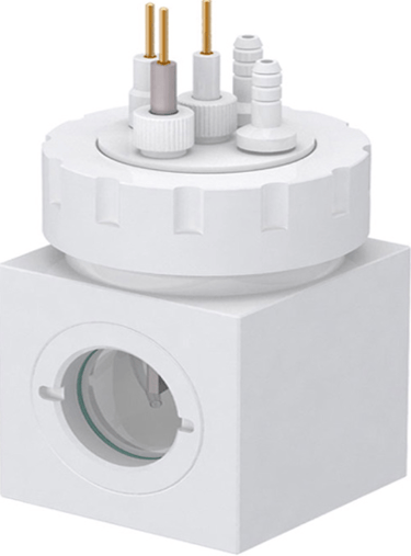
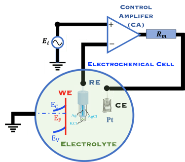
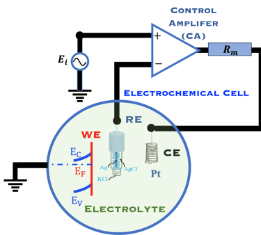
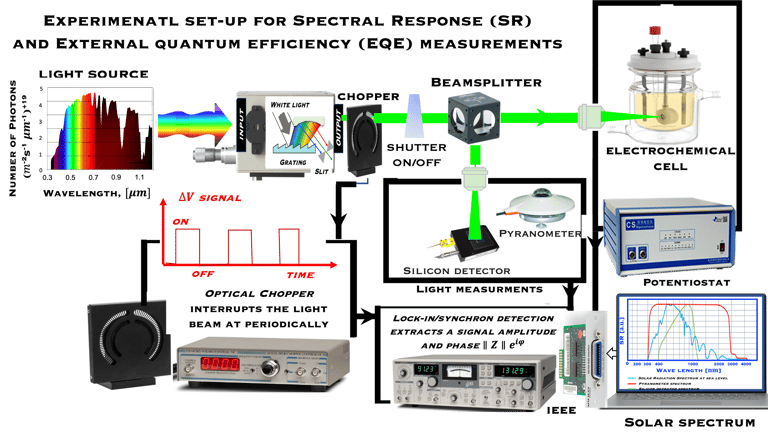
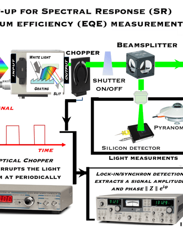
T.X.1b: (Left) - Experimental set up for spectral response (SR) and external quantum efficiency(EQE) measurements: it consists of different elements: (1) Light source (e.g. W-Hal lamp) for the illumination; (2) three electrodes PEC cell (working electrode, WE; counter electrode, CE; and reference electrode, RE (e.g. AgAgCl), (3) Potentiostat: to apply a controlled voltage and measure the dark current and photocurrent as a function of controlled potential, (4) monochromator to deliver monochromatic light with photon energy E = 𝒉𝒄/( 𝝀); (5) Look-in amplifier to receive photocurrent Iph(V) + Dark current Id(V) signals from the potentiostat and chopped light signal ∆V(t) at different 𝝀 and deliver the photocurrent IPH(𝝀). (6) a beamsplitter is used to to divide the light into two part P(𝝀)/2 hitting the PEC and P(𝝀)/2 to be measured by a reference calibrated detector, the ratio of the photocurrent to measured photon flux enable to normalise the photocurrent I(𝝀)
Electronic sketch illustrating the mode of operation of a typical potentiostat. Accurate measurements of the output current attributable to electrochemical redox reactions or other reactions, such as electrode corrosion, are the most functions of the Potentiostat
Special response (SR) of the PEC is the ratio of the photocurrent Iph(λ) generated by the PEC to the power incident on the PEC Pph(λ)


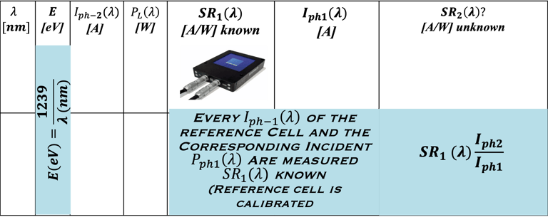
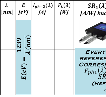
Let's consider the experimental set up T.X.1b
Each wavelength has an associated energy with a single photon E = hν = 𝒉𝒄/𝝀
The monochromator selects the wavelength 𝝀
The relation E[eV] = 1239/𝝀[nm] is used to translate the color of 𝝀 in nm into E in eV

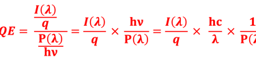
External Quantum Efficiency (EQE) of the PEC is the ratio of the number of electron (Ne) participating to the photocurrent (Iph(λ)) to the number Nph of photons hν= hc/𝝀 that hits the PEC:
We describe the properties of materials and devices, in nanometers (nm) and electron Volts (eV)
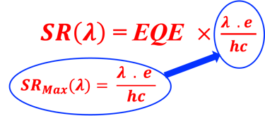

There is a clear relationship between SR and EQE


The measurement of SR and EQE consist are done as follow (see table)
Measuring a calibrated detector, Iph1(𝝀)
The monochromator selects each (𝝀) and the associated photocurrent Iph1(𝝀) [A]
A conversion table [A/W] is introduced in the program for calibration
On the other hand the unknown PEC is measured
The spectral response of PEC is SR2(𝝀) = SR1(𝝀) x Iph2/Iph1
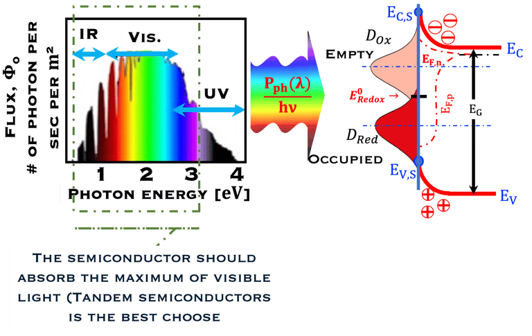
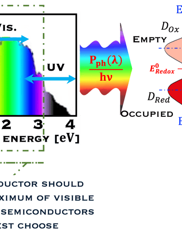
Part of photo-generated electron (Ne) are participating to the photocurrent, Iph(λ)


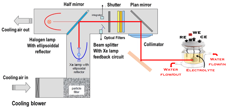
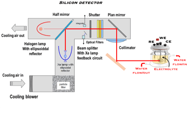
Some remarks
The best device for measuring the amount of total radiation is the so-called "PYRANOMETER"
The pyranometer gives the amount of total solar radiation that reaches the surface (directly or indirectly).
This sensor is based on the thermoelectric effect (known as the Seebeck effect)
Other photo-sensors or photo-detectors, which rely on semiconductor materials, such as silicon work based on photovoltaic process and convert light directly into electricity
There are the same principle that use several semiconductor materials with different band gap to broaden the spectral sensitivity
The Lamps for electrode illumination should provide well-stabilized and stable white light that produces a spectrum similar or close to that of the sun.
Commercially available: sun simulation source that provides AM1.5 conditions (1000 watts per square meter)
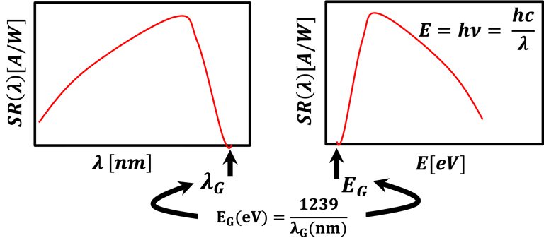
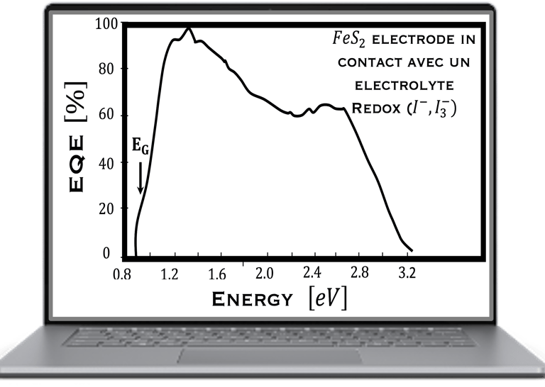
T.X.2: (Left) - Spectral response (SR) vs. wavelength (𝝀) and vs. associated energy E = hν = 𝒉𝒄/𝝀 of the incident photon. (Right) - External Quantum Efficiency (EQE) vs. Energy. the work published in ["*Ahmed Ennaoui et Al., Iron disulfide for solaZ energy conversion, Solar energy materials and solar cell, Vol. 29 (1993) 289-370"] The PEC which consists of an FeS2 photo-electrode and a carbone counter electrode in contact with a redox electrolyte is working in photovoltaic mode . EQE is a key metric for selecting new PEC materials for practical water-splitting, EQE tells us about the band gap "onset" of the material, and how well it absorbs the solar spectrum, the nature of the transition (direct or indirect) and qualitatively the recombination of charge carriers
T.X.1c: Photon ´s flux hit the photo-electrode creating electrons in the CB and holes in the VB
T.X.3: (Left) - Spectral response (SR) vs. wavelength (𝝀) and vs. associated energy E = hν = 𝒉𝒄/𝝀 of the incident photon. (Right) - External Quantum Efficiency (EQE) vs. Energy. the work published in ["*Ahmed Ennaoui et Al., Iron disulfide for solaZ energy conversion, Solar energy materials and solar cell, Vol. 29 (1993) 289-370"] The PEC which consists of an FeS2 photo-electrode and a carbone counter electrode in contact with a redox electrolyte is working in photovoltaic mode . EQE is a key metric for selecting new PEC materials for practical water-splitting, EQE tells us about the band gap "onset" of the material, the nature of the transition (direct or indirect) and qualitatively the recombination of charge carriers
The internal Quantum Efficiency (IQE) can be obtained by combining EQE and the total reflectance measurements
IQE gives information on the number of charge carriers collected versus the number of photons absorbed PEC, taking into consideration the reflection and transmission
Measurement of the reflection R( λ) and transmission T( λ) of PEC
Calculate the corrected IQE vs. reflected light for each λ [nm], and Plot IQE [%] vs. λ [nm]" or IQE vs E [eV] or both of them
IQE tell us about the wavelengths of light that are lost due to parasitic absorption
IQE measurements enable to identify the mechanisms that limit the performance that limit the photocurrent of PEC

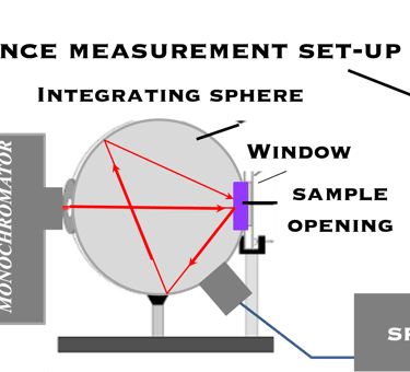
T.X.3: (Left) - Illustration of the setup for total reflection measurements and A table for most relevant data (Top). This requires an Integrating sphere to collect all reflected monochromatic light, a sample to be measured, a detector and light beam opening, several detectors and spectrometer for analysis the R(𝝀). (Right) - an example of IQE measurements published by Shude Zhang et al. in Energies 2019, 12(6), 1168, this example does not concern PEC, however, it shows the impact of the thickness and the nature of coating (ARC) on photovoltaic parameter of a solid solar cell
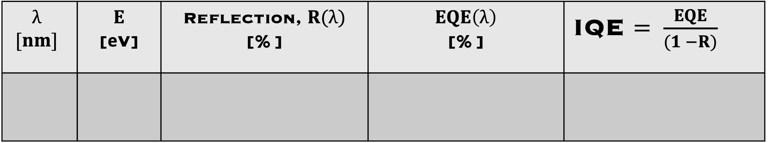
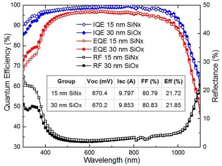
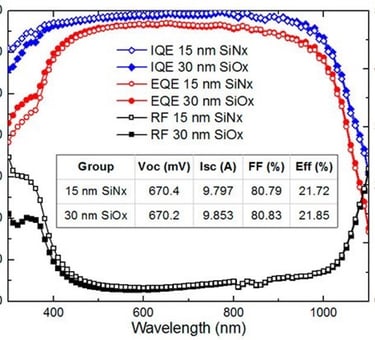
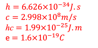


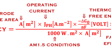
In Task XI, we discuss Solar to Hydrogen (STH) Conversion Efficiency and how to mesure the amount of hydrogen produced
We have to distinguish between quantum efficiency EQE(𝝀) and STH
We use in this task a PEC with a semiconducting electrode of N-type (anode) and a platine counter electrode
Task XI: Solar-to-Hydrogen Efficiency of Photoelectrodes
STH involves the change in Gibbs free energy which is the driving force for splitting water: ∆G°(T,p) = 237 kJ/mol
∆G°(T,p) and Redox Potential are related by -∆G°(T,p)/nF = 1.23 V, which is the minimum applied voltage for water splitting
Assuming that the only source of energy is the incident sunlight AM1.5G (no other external voltage)
Solar to Hydrogen (STH) Efficiency is defined as:
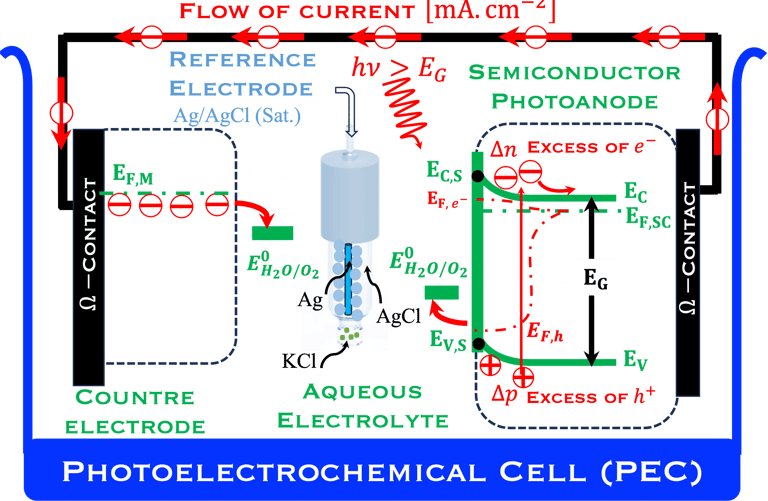
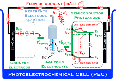

RH2 is the hydrogen production rate
An important factor, the Faraday efficiency (ηF) which is a measure of the selectivity of a specific electrochemical product during electrolysis
The selectivity of the reduction of hydrogen protons into hydrogen molecule
ηF can be seen as the electrochemical current efficiency of a particular product
Can be expressed as the product-specific charge (n x N x F) divided by the total electrical charge of the electrochemical process


Under ideal conditions, with maximum Faraday efficiency, the amount of hydrogen generated is twice the amount of oxygen in terms of the number of moles as shown in the overall water splitting reaction, and should be proportional to the electric charge passing through the solution
The Faraday efficiency equation η[%] contains
The number of moles (n) of electrons required to form one mole of product (for hydrogen, reduction of two protons to one mole of hydrogen)
The number of moles (N) of product formed during proton reduction
The Faraday (F = 96500C) which is the magnitude of electric charge per mole of electrons. F = e × NA (NA is Avogadro constant)
How to determine an accurate value of Faraday efficiency (η):
Gas chromatography (GC) is one of the most comprehensive analytical technique for quantifying gaseous products such as hydrogen.
GC offers high sensitivity, excellent separation efficiency, speed and automation, making it the preferred choice for research and development


The Faraday efficiency equation η[%] contains
ne: Number of moles of electrons needed to obtain one molecule of product
x: ppm of gaseous products formed
T = 298.15K Temperature
F = 96500 C: Faraday constant
(R) = 8.314 J per Kelvin per mole: gas constant
P: 101325 Pa: Standard atmospheric pressure
I: Current density at the time of sampling
Summary: Experimental routine to follow
We consider the following: Amount of a given gas Np mol
Size of the sample loop used in the gas chromatograph V
Amount of gas (n) to be measured (Ideal gas law: n = PV/RT), at the conditions of pressure P and temperature T
The analys shows a detected product (𝑥) in ppm,
The amounts of moles of the gaseous product will be: (Np = 𝑥 . n / 1000000)
The number of electron moles required to obtain a quantity of protons reduced to a hydrogen product is:
𝑁𝑝 × the number of electron moles required to obtain one mole of product (e)n
The total number of electron moles transferred during the sampling time 𝑡 is:
𝑁𝑝 × the number of electron moles required to obtain one mole of product (e)n: I x t/F = e(t)
(𝑡 = V/flow rate) The time required to fill the volume of the sample loop
I is the current during the sampling time t
The experimental set up is shown in figure T.XI.2 below


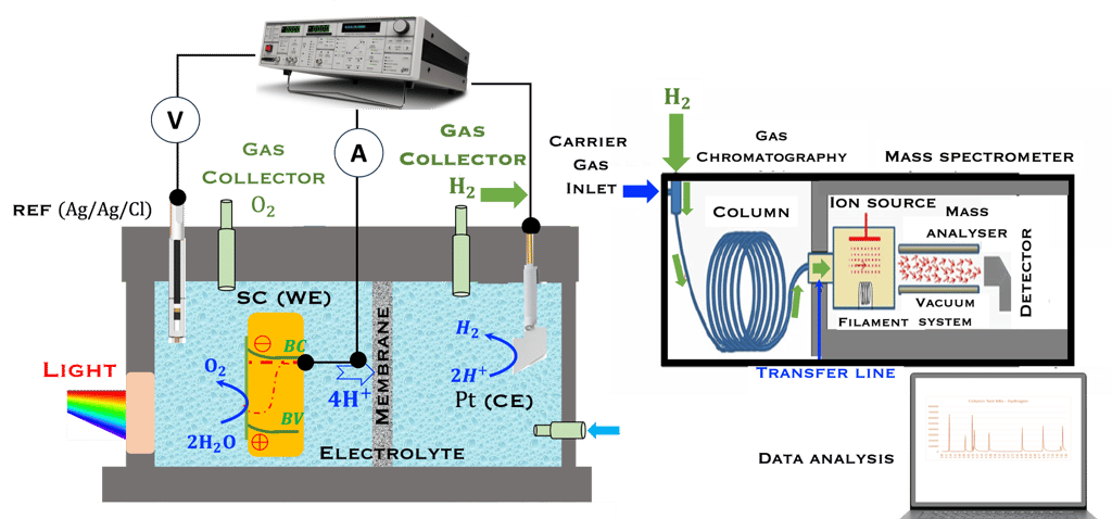
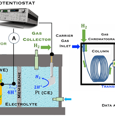
T-XI.2: (Left) - schematic of PEC with N-type semiconductor as working electrode (Anode: WE), Metal platine as counter electrode (Cathode: Pt), and reference electrode (Ag/AgCl). The PEC is equipped with a system for gas collection, a quarz window for illumination, and a potentiostat for controlling the potential potential. (Right) - A simplified diagram of a gas chromatograph–mass spectrometer showing: inlets for Hydrogen and for carrier gas, analytical column (GC), Mass spectrometer and data analysis tools.
Credit: Illustration of Gas Chromatography–Mass Spectrometry adapted from: source: Emwas, Abdul-Hamid & Al-Talla, Zeyad & Kharbatia, Najeh. (2015). Sample Collection and Preparation ofBiofluids and Extracts for Gas Chromatography–Mass Spectrometry. Methods in molecularbiology (Clifton, N.J.). 1277. 75-90. 10.1007/978-1-4939-2377-9_7
Sources: Data and experimental routine adapted from Nilutpal Dutta, Debabrata Bagchi, Geetansh Chawla, et al ACS Energy Lett. 2024, 9, 323−328
Sources: Data and experimental routine adapted from Nilutpal Dutta, Debabrata Bagchi, Geetansh Chawla, et al ACS Energy Lett. 2024, 9, 323−328
External Quantum Efficiency and Spectral response as defined in previous Task
Task XII: Solar-to-Hydrogen process: discussion of I-V and C-V characteristics
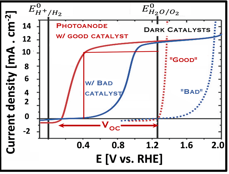
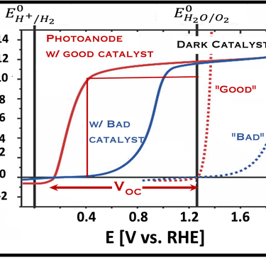
Figure XII.1 (Left) illustrate a linear sweep voltammetry
The electrodes are connected to the potentiostat, and the experimental parameters are selected through a software
The potential range is fixed and the voltage is swept from left to the right and vis-versa
The voltammogram enable to collect information about the reactions mechanism occurring at the surface of the WE, and the kinetics of these reactions
Figure XII.1 (Right) shows the I-V characteristics after the paper entitled Solar Water Splitting Cells [Michael G. Walter, et al. Chem. Rev. 2010, 110, 6446–6473]
In this work the potential of the WE is given versus RHE (Reversible Hydrogen electrode)
The I-V characteristics illustrate the effects of surface catalysts on the photo-electrodes in the dark and under illumination
The effect of “good” catalyst, shows that only a voltage of ca. 100 mV is enough to produce a current density of ∼10 mA per SQCM, whereas for a “bad” catalyst ∼600 mV is needed to produce the same current density
I-V with good fill factor and open-circuit voltage (Voc) produced by the use of catalyst is visible and enhances the efficiency
The catalysts and Electrocatalysts play a crucial role by overcoming the kinetic energy barriers for electro- chemical reactions of water, andr increasing the efficiency of OER and HER
To understand the I-V characteristics, we have to go back to the experimental set up measurements can be performed in the dark and under illumination
Linear sweep voltammetry technique can be typically used, it consists of applying a controlled potential to the working electrode (WE) (here the photoanode) versus SHE
WE is swept linearly versus time V = V(t) and the resulting current is measured between WE and a couter electrode (here a platinum electrode)
The current density I[mA/SQCM] is plotted as a function of this potential V vs. SHE.
All experiments are monitored with the potentiostat which has complete control over the applied potential
Figure XIII.1 (Left) shows an illustration with three-electrode configuration a reference electrode (SHE), a metal wire (Platine, Pt) as the counter electrode (CE). and an N-type semiconductor as positive anode under illumination
The accurate measurements under illumination are typically performed with a class AAA solar simulatorto provide a good match to the AM1.5 spectrum

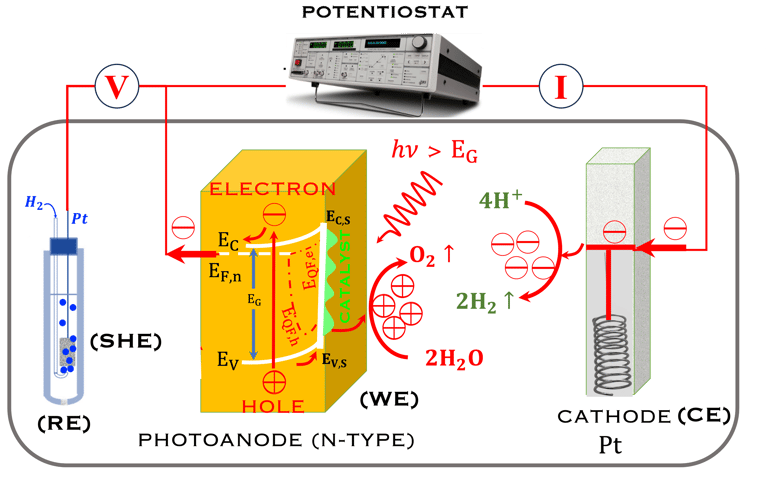
At the anode: OER
At the cathode: HER
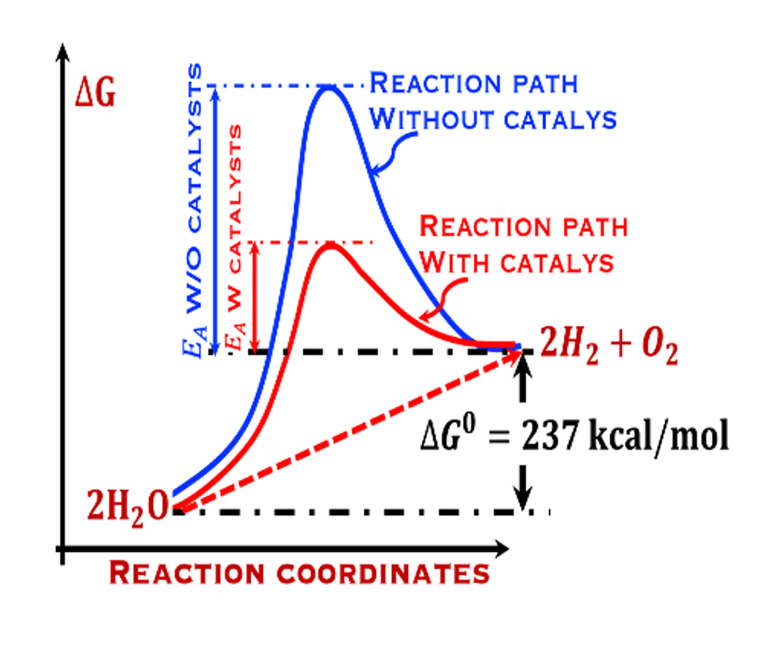
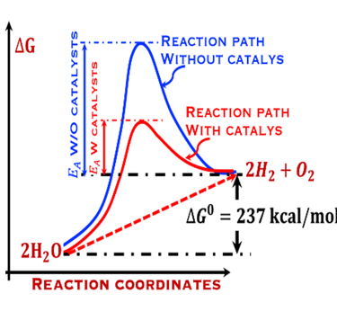
Schematic adapted from the paper published by Wang et al. in Nano Convergence entitled "Hydrogen production from water electrolysis". There are fundamental conditions namely semiconductor electrode must generate two electron-hole pairs per water molecule to produce hydrogen, and four electron-hole pairs per water molecule to produce oxygen (see HER and OER and electrochemical reactions). Furthermore the catalysts are conceived to reduce the activation energy barrier for water splitting as shown in red color
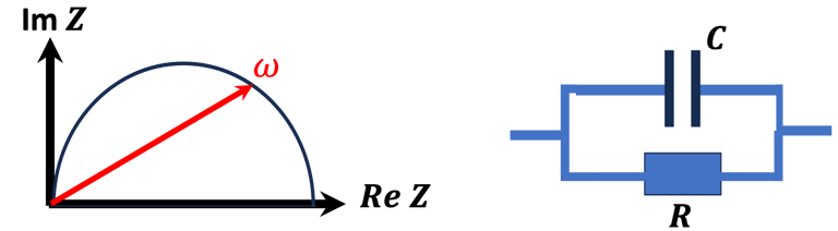
A "Nyquist Plot" representing the equivalentcircuit of electrochemical impedance (simple one "time constant)
Each point on the Nyquist Plot is the impedance at one frequency

The impedance presented by a complex number:
Eulers relationship:


Ohm's Law enable to calculate the impedance as:
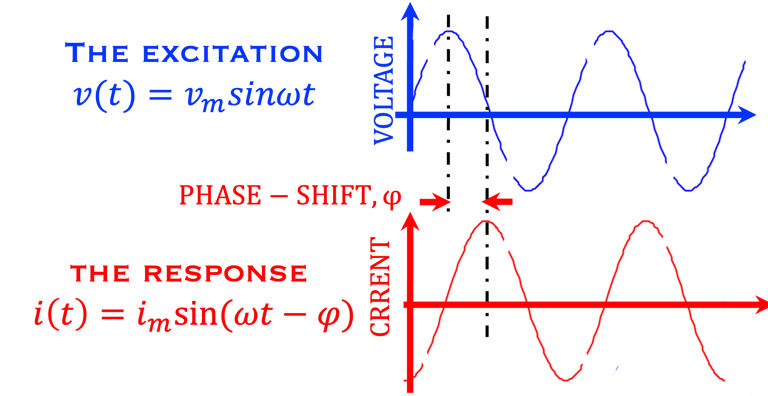
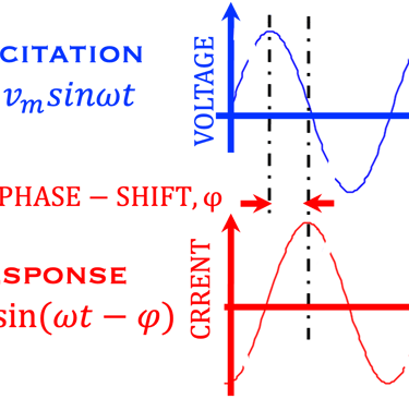
Electrochemical Impedance measurements
Electrical resistance mesures the ability to resist the flow of electrical current R[Ω] = voltage/current
Electrochemical systems exhibit much more complex behavior and the measurements are also complex
The technique consists of providing a small (AC) modulation of the potential to the working electrode in addition to DC potential as we used for "cyclic Voltammetry"
the current response is also a small AC sinusoidal potential having the same frequency but shifted in phase
A range of frequency can be used resulting in a complex impedance known as Nyquist plot, with the real component in x-axis and the imaginary component in the y-axis
A fitting the impedance program can provide an equivalent circuit, processes at the photo-electrode in th dark and under illumination
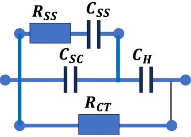
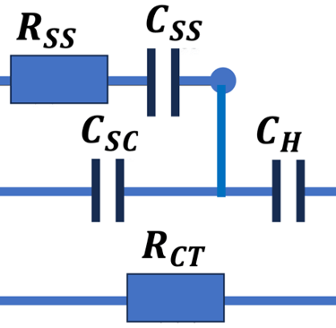
(Left) - simplified equivalent circuite adapted from Journal of Physics D: Applied Physics, (2021) 54 (19). 54 269601, by María del Carmen Mejia al. on the analysis of the physical photoelectrochemical properties of Si(p)/SiC:H(p) for solar water splitting. It consists of surface state component (Rss, Css) component, in parallel with the space charge Css and the helmoltz component. RCT that reprensents the charge transfer resistance. (right) - Illustration of various layers, their potentials, and their widths
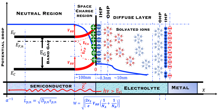
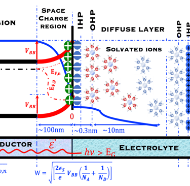
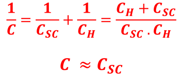
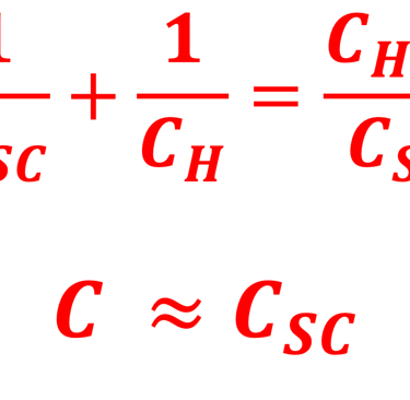
Solid/electrolyte Surface states and equivalent circuit
Atoms located on the surface of the semiconductorhave the so-called dangling bonds that createmultitude of defect levels distributed throughoutthe band gap
Dangling bonds in semiconductor (e.g. Si, III-V, II-VI, "semiconductor compounds with d orbital") in contact with an electrolyte create surface states that can influence the process of water splitting
The electrical charges consists of a Helmholtz layer (QHL ), the neglited diffusion charge and a space charge in the semiconductor side (Qsc )
The Helmholtz layer (QHL ) contains an inner Helmholtz layer (IHL) and outer Helmholtz layer , both depending on the adsorption of water molecules, the excess charges stored at the electrode, and the ions in the electrolyte.
In most studied case the capacitance of charge space (Csc) is small compared to the Helmholtz layer (CH) i.e Csc << CH
Electrochemical Impedance Spectroscopy (EIS
The technique consists of providing a small (AC) modulation of the potential to the working electrode in addition to DC potential as we used for "cyclic Voltammetry"
The resulting modulated current is a complex impedance
A range of frequency can be used resulting in a complex impedance known as Nyquist plot, with the real component in x-axis and the imaginary component in the y-axis
A fitting the impedance program can provide an equivalent circuit, processes at the photo-electrode in th dark and under illumination
How do Impedance measurements work?
The potentiostat enable to control the voltage between (WE) and (RE) and the resulting current is measured between(WE) and ((CE)
The lock-in amplifier provides high resolution measurementsover several orders of magnitude and frequency
A sinusoidal waveform v(t) is applied at a set frequency [μHz - MHz] and the resuting AC current i(t) with a phase shift is measured
The illustration below, shows:
the small ac v(t) modulation of the dc potential V(t) (on the screen) applied to the working electrode
The two AC signals v(t) and i(t) shifted in phase and the corresponding Complex impedance
Linear speep voltage of the potentiostat enable to change the band binding (we suppose Evs and Ecs fixed) enabling the measurement of the flat band potential Vfp
Csc can be measured at frequency range where only Csc is affected by changing the potential
Mott-Schottky plot can be obtained from the following equation:
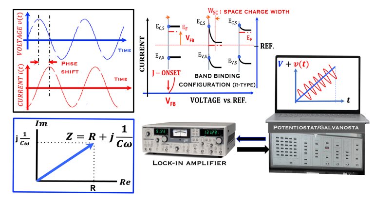
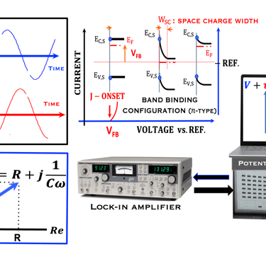


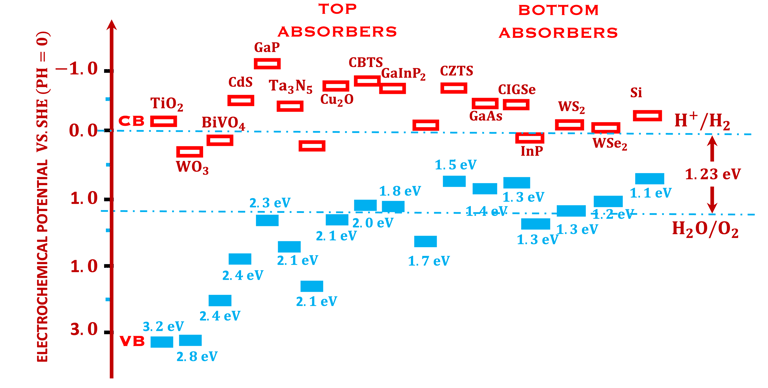
The flat band potential is determined from the x-axis intercept of the the linear slop
The band edge positions (Ecs, Evs) with respect to the redox potentials of water splitting (here for pH = 0) can be deduced using the concentration n and p of charge carriers
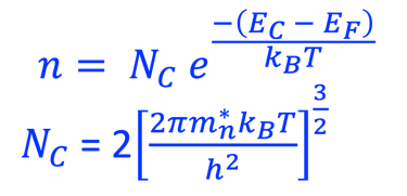
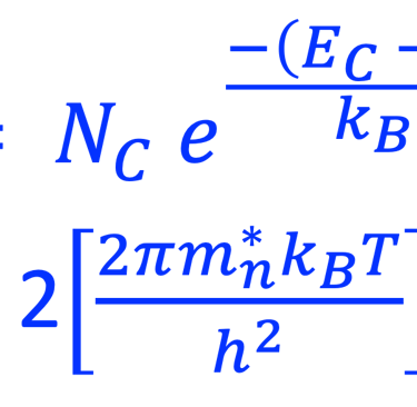
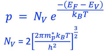

Below the results from an interesting work untiled "Roadmap on solar water splitting: current status and future prospects" published by by Sheng Chu et al. in IOPscience several wide and narrow band gap materials are tested as photoelectron to be used as top and bottom absorbers, in PEC for water splitting
A Mott-Schottky plot of PEC solar cell (Photovoltaic mode), [my work published in Solar Energy Materials 14 (1986) 461-474]
A tandem PEC water splitting system based on different photoelectrode absorbers to achieve Artificial photosynthesis
Different type of absorbers that have different bandgaps are put together and allows more photons to be absorbed by the PEC
Photons that are not absorbed by a top large bandgap absorber are transmitted and harvested by the bottom low bandgap absorber
Light absorption and energy band matching are the key points to enhance the solar-to-hydrogen (STH) efficiency
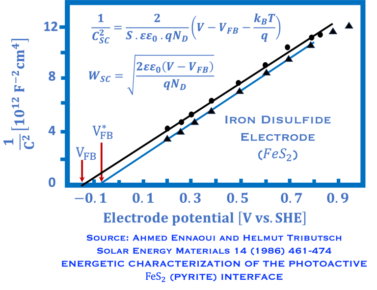
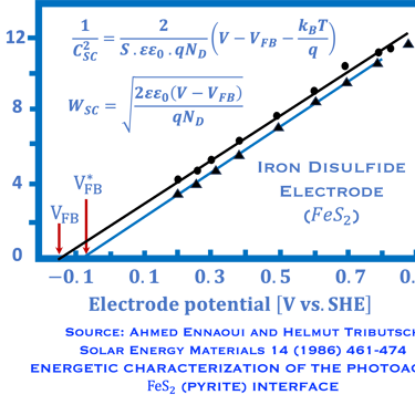
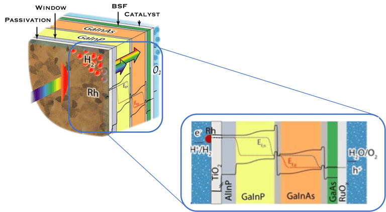
Illustration Rh/TiO2/Multijunction (AlInP/GaInP/GaInAs/GaAs)/RuOx tandem as record PEC device for unassisted water splitting.
sources: W.-H. Cheng, M. H. Richter, M. M. May, J. Ohlmann, D. Lackner, F. Dimroth, T. Hannappel, H. A. Atwater, H.-J. Lewerenz, ACS Energy Lett. 2018, 3, 1795-1800 // Sol. RRL 2022, 6, 2200181//Sol. RRL 2024, 8, 2301047
ACS Energy Lett. 2020, 5, 470−476
Thesis (CALIFORNIA INSTITUTE OF TECHNOLOGY Pasadena, California)
The work published by Wen-Hui Cheng et al. on highly Efficient unassisted photoelectrochemical device based on photovoltaic tandem heterojunctions including efficient catalyst nanoparticles
The PEC device works under simulated AM 1.5G irradiation, and shows a record solar-to-hydrogen efficiencies of 19.3 and 18.5% in acidic and neutral electrolytes
One of the co-authors of the article, Prof. Dr. Thomas Hannappel, presented a webinar (available here).
Here is the architecture of the PEC cell presented by Thomas
GREEN HYDROGEN AND SOLAR FUEL WITH ARTIFICIAL PHOTOSYNTHESIS
BY THOMAS HANNAPPEL
Head of the department “Fundamentals of Energy Materials”
Dean of the Master course “Renewable Energy Techniques” at the Institute of Physics, Technische Universität (TU) Ilmenau
Task XIII. Fossil Fuels vs. Green Hydrogen: Energy Efficiency and Environmental Impact


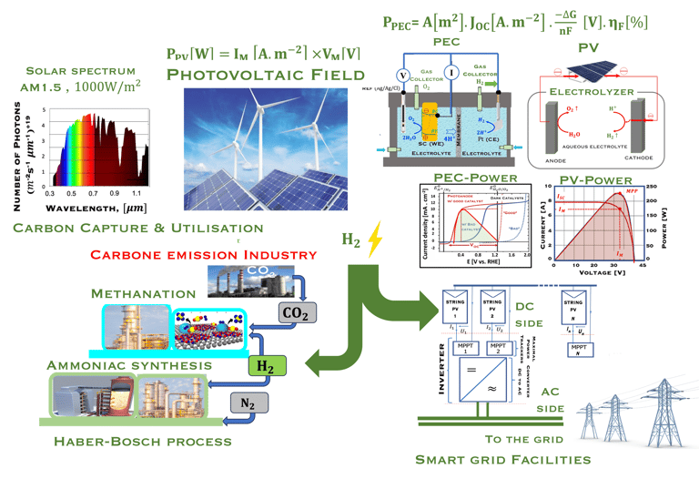
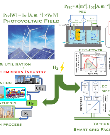
We talk about "Green Hydrogen" when we use a renewable source of electricity to make it through electrolytic decomposition of water
Green hydrogen is produced from renewable energy (e.g. Photovoltaic electricity) without releasing carbone dioxide
Green hydrogen is fuel that can combusts in the industry processes without producing any carbon footprint, thus it has the potential to decarbonize challenging industries such as steel production
Green hydrogen can power vehicles equipped with hydrogen fuel cells, which convert energy to electricity and water and can be more efficient than internal combustion engines (Fuel cells can be 3 times more efficient)
Green hydrogen still need a lot of investment for large scale in order to be economically competitive compared to fossil fuels which is the primary source for power generation today
Most of the studies demonstrate the causal link between the man-made GHG emissions and global warming
sources: [ https://robbieandrew.github.io/GCB2021/ ] and [ Earth Syst. Sci. Data, 17, 965–1039, 2025 https://doi.org/10.5194/essd-17-965-2025 ]


Blue hydrogen: the alternative
To align with current regulations, the industrial sector is in the way to integrate technologies called Carbon Capture, Utilization, and Storage (CCUS)
A substantial decrease in CO2 emissions from industrial processes and a reduction of CO2 from the atmosphere is a must
The process "called steam methane reforming" produces hydrogen and carbon monoxide (CO) as byproduct
methane (CH4) reacts with steam (H2O) to produce synthetic gas (syngas), which consists of (CO) and hydrogen (H2) according to the chemical reaction
𝐶𝐻4 + 𝐻2𝑂(𝑠𝑡𝑒𝑎𝑚) → 𝐶𝑂 + 3𝐻2 with CO:H2 ratio of 1:3
A process called "water-gas shift reaction" enable extra generation of hydrogen where (CO) reacts with more steam, as follow:
𝐶𝑂 + 𝐻2𝑂(𝑠𝑡𝑒𝑎𝑚) → 𝐻2 + 𝐶𝑂2
Hydrogen from steam methane reforming is considered as “blue hydrogen” as soon as CO2 is captured and stored, then
A sustainable process that integrates Green Hydrogen in the fabrication of methane and the production of ammonia is shown in (T.XIII.1a)
Option: Green Hydrogen from electrolysis with nitrogen of the atmosphere in the Haber-Bosch process to produce ammonia
Option: Green Hydrogen from electrolysis with Carbone dioxide from the industry to produce methane
Comparing steam methane reforming which generate CO2 and the process generates a pure stream of hydrogen and oxygen with zero emission when the electricity provided comes from renewable sources, we have to choose either green hydrogen or at least blue Hydrogen
The list is long and We rely on you to complete it exhaustively
T.XIII.1a: (Top) - The Illustration shows the use excess electricity from renewable sources to power electrolyzers for indirect production of green hydrogen. Furthermore a Photoelectrochemical PEC system to produce green hydrogen directly (under R&D). Green hydrogen can be injected together with carbone dioxide (CO2), to be fixed in the production of methanol (methanation) and the fabrication of ammoniac (Haber-Bosch process). I quote from this message from IEA "Smart grid technologies can help to manage this transition while reducing the need for costly new grid infrastructure, and can also help to make grids more resilient and reliable Source: https://www.iea.org/energy-system/electricity/smart-grids "
T.XIII.1b: (Bottom) -Carbone based Hydrogen production and consumption [adapted from the paper of S. Shiva Kumar and Hankwon Lim, published in Energy Reports Volume 8, November 2022, Pages 13793-13813]. Currently green hydrogen through electrolysis represents only ca. 4% old production
Task XIV. Factors influencing the Levelized Cost Of Hydrogen (LCOH): Morocco case
Introduction - Morocco has a strong track record in renewable energy, with abundant wind and solar resources at different place exceptionally in Moroccan Sahara. Political momentum has built up in Morocco to become a leader in green hydrogen production, and the country has ambitious goals for generating half of its electricity from renewables by 2030-2050, This energy transition includes important steps on the development of green hydrogen facilities toward energy system that uses hydrogen produced from renewable energy sources and the integration of green hydrogen into the industry, transportation sector. trade agreements exist between Morocco and several countries, I quote "Morocco World News" (Five major investors have been selected to develop six projects worth $31.9 billion), end of quote. Among the countries that support Morocco, we would firstly mention Germany, a country that is highly advanced in terms of knowledge and hydrogen green technology. The energy partnership with Germany dates back to 2012 to promote the energy transition. One of Morocco's assets is its close ties with Europe and unambiguous diplomatic and trade relations. However, challenges remain building infrastructures ensuring the efficient integration, storage, and distribution of renewable energy. For this purpose, moroccan government announced various measures to accelerate the development of renewable energy technologies through the building of new infrastructures and to manage a long-term energy security of the country. Another barrier is water scarcity, and the limited supply of fresh water required for hydrogen electrolysers.
Electrolyzer prices [$ per kW of hydrogen produced for a given current density]